
Global Silicon on Insulator (SOI) Market Outlook to 2030
Region:Global
Author(s):Shivani Mehra
Product Code:KROD1218
December 2024
93
About the Report
Global Silicon on Insulator (SOI) Market Overview
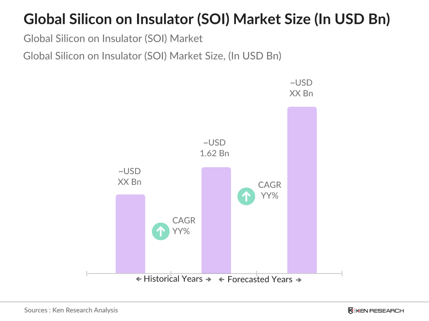
- The global Silicon on Insulator (SOI) market, currently valued at USD 1.62 billion, is driven by technological advancements, primarily in the semiconductor and microelectronics sectors. This growth is attributed to the rising demand for high-performance and energy-efficient electronics, as well as the expansion of 5G infrastructure and automotive applications. These developments have accelerated the adoption of SOI technology, enhancing power efficiency, processing speed, and device performance. Furthermore, the SOI markets growth is fostered by continuous innovation in semiconductor fabrication technologies.
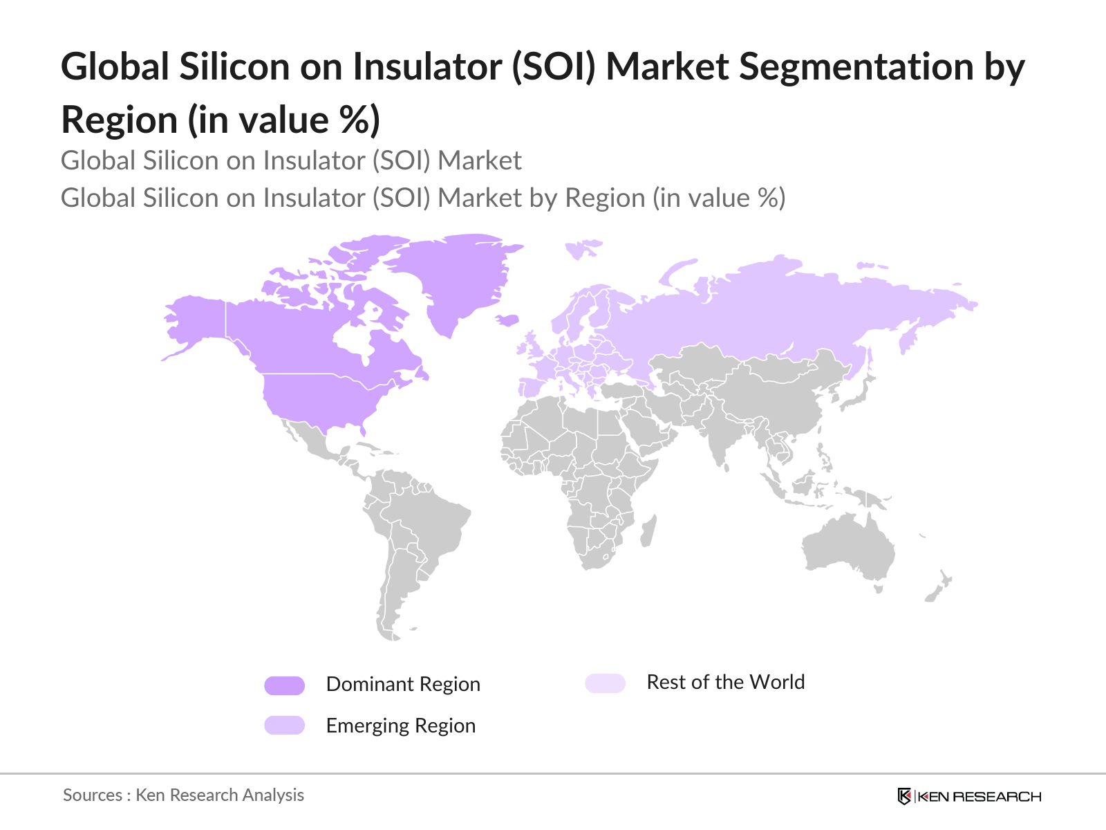
- In the SOI market, regions like North America and Asia Pacific are dominant due to their robust semiconductor manufacturing and research facilities. North America, with its advanced technological landscape, is a leader in SOI technology development, while Asia Pacific, particularly countries like Japan, China, and South Korea, has established a strong production base. The presence of major electronic manufacturing hubs and a growing demand for electronic devices contribute to the dominance of these regions in the SOI market.
- The Indian government has implemented a $10 billion Production Linked Incentive (PLI) scheme to support the growth of the semiconductor manufacturing industry. Announced in 2023, this initiative provides financial support and subsidies for establishing semiconductor fabrication facilities and design capabilities. This incentive program aims to position India as a global semiconductor hub and promote the adoption of advanced technologies, including Silicon on Insulator (SOI) wafers, in various industries.
Global Silicon on Insulator (SOI) Market Segmentation
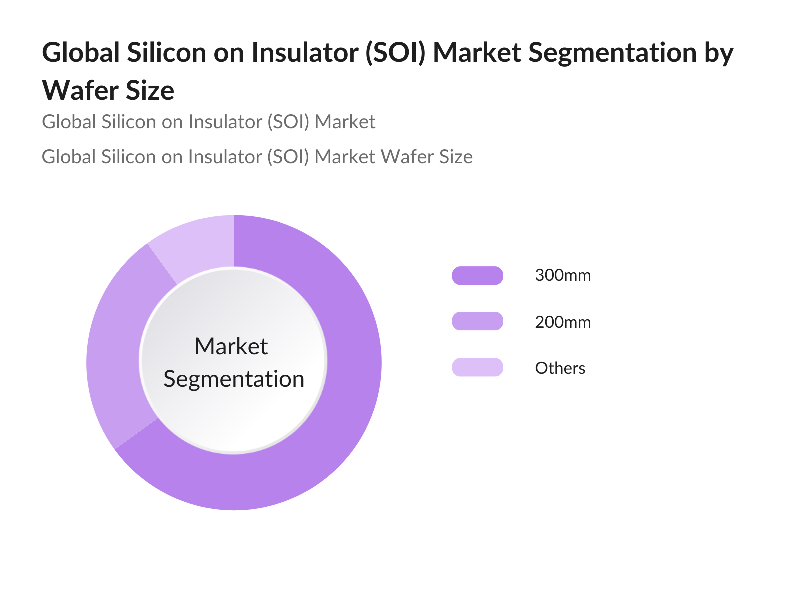
By Wafer Size: The SOI market is segmented by wafer size into 200mm, 300mm, and other sizes. Recently, the 300mm segment has dominated the wafer size segmentation in the SOI market, primarily because it allows higher yield and cost efficiency, which are essential for high-volume semiconductor applications. The growing adoption of 300mm wafers for use in high-performance computing, data centers, and automotive electronics has strengthened its position as the preferred wafer size for SOI production.
By Region: The SOI market spans North America, Europe, Asia Pacific, Middle East & Africa, and Latin America. North America has a dominant market share due to its established semiconductor industry and advancements in SOI technology. Additionally, Asia Pacific is witnessing rapid growth, fueled by increasing investments in semiconductor manufacturing facilities in China, Japan, and South Korea, making it a critical region for SOI technology in consumer electronics and automotive applications.
Global Silicon on Insulator (SOI) Market Competitive Landscape
The global SOI market is dominated by a few key players who leverage their technological expertise and market presence to drive growth. These companies continually innovate to address the high-performance demands of consumer electronics, automotive, and data-intensive applications.
Global Silicon on Insulator (SOI) Market Analysis
Market Growth Drivers
- Technological Advancements (FD-SOI, RF-SOI): The global semiconductor industry has witnessed significant technological advancements, particularly in Fully Depleted Silicon on Insulator (FD-SOI) and Radio Frequency Silicon on Insulator (RF-SOI) technologies. FD-SOI technology enhances performance and reduces power consumption in microprocessors and System-on-Chip (SoC) designs, making it ideal for mobile and IoT applications.
- Increasing Adoption in Electronics (5G, IoT, Data Centers): The proliferation of 5G networks, Internet of Things (IoT) devices, and data centers has significantly increased the adoption of SOI technology. According to the International Telecommunication Union (ITU), by the end of 2023, there were approximately 1.5 billion 5G subscriptions worldwide, necessitating advanced semiconductor components for enhanced connectivity. The IoT sector has also expanded, with the International Data Corporation (IDC) reporting over 30 billion connected devices globally in 2023, all requiring efficient and reliable semiconductor solutions.
- Rise in Demand for Energy-Efficient Solutions: The global emphasis on energy efficiency has propelled the demand for SOI technology in semiconductor manufacturing. The International Energy Agency (IEA) reported that in 2023, global electricity consumption reached 25,000 terawatt-hours, with a significant portion attributed to electronic devices and data centers. SOI technology offers reduced power leakage and lower energy consumption, aligning with global energy efficiency goals.
Market Challenges:
- High Cost of SOI Wafer Production: The production of SOI wafers involves complex processes and advanced materials, resulting in higher manufacturing costs compared to traditional silicon wafers. The U.S. Department of Commerce reported that in 2023, the average cost of producing a 300mm SOI wafer was significantly higher than that of a bulk silicon wafer, which impacts the overall cost structure for semiconductor manufacturers. This cost disparity poses a challenge for widespread adoption, particularly among applications and markets where cost sensitivity is a critical factor.
- Complexity in Fabrication Processes: The fabrication of SOI-based devices requires specialized equipment and processes, adding complexity to semiconductor manufacturing. The Semiconductor Industry Association (SIA) noted in its 2023 report that integrating SOI technology necessitates additional steps such as layer transfer and bonding, which can increase production time and potential for defects. This complexity can deter manufacturers from adopting SOI technology, particularly when existing bulk silicon processes are well-established and cost-effective.
Global Silicon on Insulator (SOI) Market Future Outlook
Over the next few years, the SOI market is anticipated to grow significantly, driven by advancements in semiconductor technology and the expansion of applications in IoT, automotive, and 5G networks. The focus on enhancing energy efficiency and device performance is expected to increase the adoption of SOI wafers, especially in emerging markets in Asia Pacific and the Middle East. Increasing collaborations between SOI manufacturers and technology firms will likely foster further innovation, supporting the sustained growth of the SOI industry.
Market Opportunities:
- Expansion in Emerging Markets (Asia Pacific, Middle East): Emerging markets, particularly in the Asia Pacific and Middle East regions, offer substantial growth opportunities for the SOI market. The World Bank reported that in 2023, countries like India and Vietnam experienced strong economic expansion, with notable increases in GDP that signal a favorable environment for investment. This economic growth is accompanied by rising investments in semiconductor manufacturing and technology infrastructure, further bolstering the demand for advanced semiconductor technologies in these regions.
- Growing Applications in Automotive Semiconductors: The automotive industry is increasingly adopting SOI technology for applications in advanced driver-assistance systems (ADAS), electric vehicles (EVs), and in-vehicle infotainment systems. The International Organization of Motor Vehicle Manufacturers (OICA) reported that in 2023, global EV sales reached 10 million units, a 40% increase from the previous year, highlighting the growing demand for advanced semiconductor components.
Scope of the Report
|
By Wafer Size |
200mm 300mm Others |
|
By Product Type |
Fully Depleted SOI (FD-SOI) Partially Depleted SOI (PD-SOI) Power SOI |
|
By Application |
Consumer Electronics Automotive Industrial Datacom & Telecom Others |
|
By Technology |
Smart Cut Bonding Layer Transfer |
|
By Region |
North America Europe Asia Pacific Middle East & Africa Latin America |
Products
Key Target Audience
Semiconductor Manufacturing Companies
SOI Wafer Suppliers
Automotive OEMs and Tier 1 Suppliers
Consumer Electronics Manufacturers
Datacom & Telecom Providers
Investments and Venture Capitalist Firms
Government and Regulatory Bodies (e.g., U.S. Environmental Protection Agency, Japans Ministry of Economy, Trade and Industry)
Technology Research Institutes
Companies
Players Mention in the Report
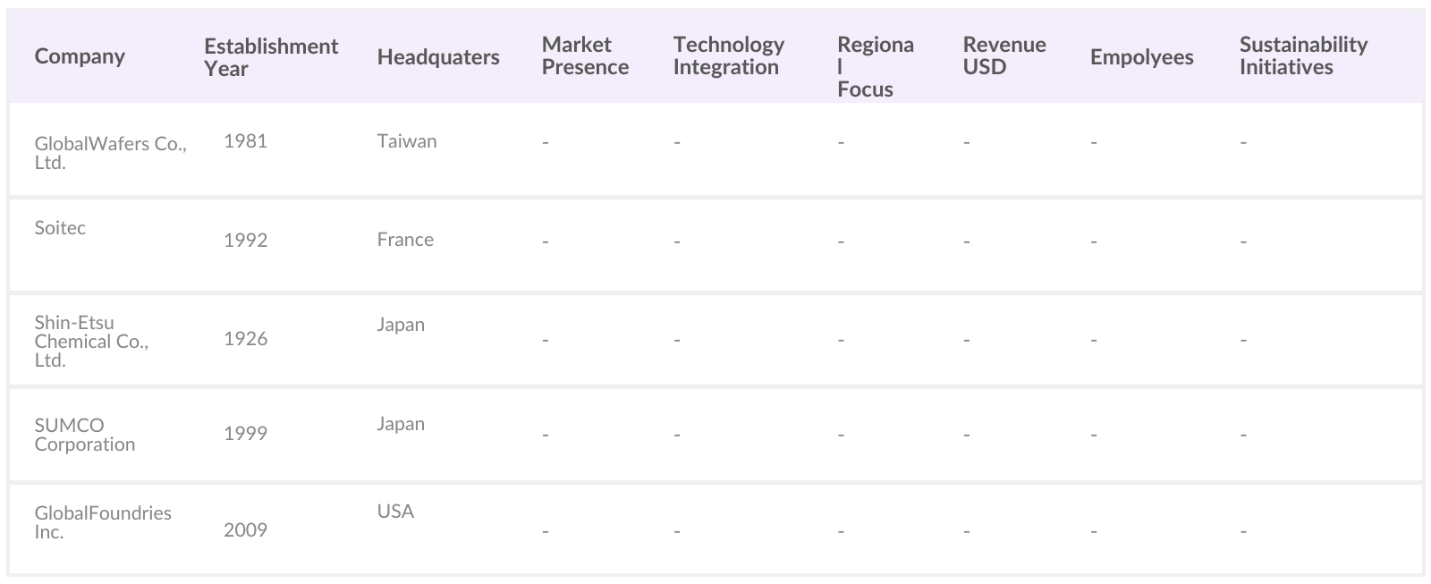
GlobalWafers Co., Ltd.
Shin-Etsu Chemical Co., Ltd.
Soitec
SUMCO Corporation
Simgui
Murata Manufacturing Co., Ltd.
GlobalFoundries Inc.
STMicroelectronics N.V.
NXP Semiconductors
United Microelectronics Corporation (UMC)
Samsung Electronics Co., Ltd.
Tower Semiconductor Ltd.
MagnaChip Semiconductor Corporation
Taiwan Semiconductor Manufacturing Company Limited (TSMC)
Skyworks Solutions, Inc.
Table of Contents
01. Global Silicon on Insulator (SOI) Market Overview
Definition and Scope
Market Taxonomy
Market Growth Rate
Market Segmentation Overview
02. Global Silicon on Insulator (SOI) Market Size (in USD Billion)
Historical Market Size
Year-on-Year Growth Analysis
Key Market Developments and Milestones
03. Global Silicon on Insulator (SOI) Market Dynamics
Growth Drivers
Technological Advancements (FD-SOI, RF-SOI)
Increasing Adoption in Electronics (5G, IoT, Data Centers)
Rise in Demand for Energy-Efficient Solutions
Market Challenges
High Cost of SOI Wafer Production
Complexity in Fabrication Processes
Opportunities
Expansion in Emerging Markets (Asia Pacific, Middle East)
Advancements in SOI-based Photonics
Market Trends
Shift Towards Ultra-Thin SOI Wafers
Growing Applications in Automotive Semiconductors
Regulatory Landscape
Environmental Regulations on Semiconductor Manufacturing
Compliance with Semiconductor Industry Standards
04. Global Silicon on Insulator (SOI) Market Segmentation
By Wafer Size (in Value %)
200mm
300mm
Others
By Product Type (in Value %)
Fully Depleted SOI (FD-SOI)
Partially Depleted SOI (PD-SOI)
Power SOI
By Application (in Value %)
Consumer Electronics
Automotive
Industrial
Datacom & Telecom
Others
By Technology (in Value %)
Smart Cut
Bonding
Layer Transfer
By Region (in Value %)
North America
Europe
Asia Pacific
Middle East & Africa
Latin America
05. Global Silicon on Insulator (SOI) Market Competitive Analysis
Detailed Profiles of Major Companies
GlobalWafers Co., Ltd.
Shin-Etsu Chemical Co., Ltd.
Soitec
SUMCO Corporation
Simgui
Murata Manufacturing Co., Ltd.
GlobalFoundries Inc.
STMicroelectronics N.V.
NXP Semiconductors
United Microelectronics Corporation (UMC)
Samsung Electronics Co., Ltd.
Tower Semiconductor Ltd.
MagnaChip Semiconductor Corporation
Taiwan Semiconductor Manufacturing Company Limited (TSMC)
Skyworks Solutions, Inc.
Cross Comparison Parameters (Wafer Size Capability, Headquarters, Inception Year, R&D Spending, Revenue, Product Portfolio Diversity, Manufacturing Locations, Strategic Partnerships)
Market Share Analysis
Strategic Initiatives
Mergers and Acquisitions
Investment Analysis
Venture Capital Funding
Government Grants
Private Equity Investments
06. Global Silicon on Insulator (SOI) Market Regulatory Framework
Environmental Standards
Compliance Requirements
Certification Processes
07. Global Silicon on Insulator (SOI) Future Market Size (in USD Billion)
Future Market Size Projections
Key Factors Driving Future Market Growth
08. Global Silicon on Insulator (SOI) Future Market Segmentation
By Wafer Size (in Value %)
By Product Type (in Value %)
By Application (in Value %)
By Technology (in Value %)
By Region (in Value %)
09. Global Silicon on Insulator (SOI) Market Analysts Recommendations
TAM/SAM/SOM Analysis
Customer Cohort Analysis
Marketing Initiatives
White Space Opportunity Analysis
Disclaimer Contact UsResearch Methodology
Step 1: Identification of Key Variables
The research begins by mapping the SOI markets stakeholder ecosystem, identifying crucial factors such as wafer size, technology, and end-use applications. Data sources include both proprietary and publicly available databases to ensure accuracy.
Step 2: Market Analysis and Construction
Historical data from the SOI market is analyzed to evaluate industry growth, market penetration, and revenue patterns. Special attention is given to production output, market demand, and technological advancements influencing the market.
Step 3: Hypothesis Validation and Expert Consultation
Hypotheses are developed based on initial findings and then validated through direct consultations with industry experts. These insights help in refining market forecasts and validating revenue projections.
Step 4: Research Synthesis and Final Output
A final synthesis involves consolidating data from multiple semiconductor and SOI manufacturers, validating trends, and fine-tuning insights. This phase ensures the report accurately reflects the SOI markets dynamics, challenges, and opportunities.
Frequently Asked Questions
01. How big is the Global Silicon on Insulator (SOI) Market?
The global Silicon on Insulator (SOI) market is valued at USD 1.62 billion, driven by growing demand for energy-efficient semiconductor solutions across electronics, automotive, and telecom sectors.
02. What are the key growth drivers in the Global SOI Market?
Major growth drivers include increasing 5G infrastructure deployment, advancements in IoT applications, and demand for high-performance, low-power semiconductor devices.
03. Who are the major players in the Global SOI Market?
Key players in the market include Soitec, Shin-Etsu Chemical Co., Ltd., GlobalWafers Co., Ltd., SUMCO Corporation, and GlobalFoundries Inc., all of whom hold significant market influence due to their technological expertise and product portfolios.
04. What challenges exist in the Global SOI Market?
Key challenges include high production costs of SOI wafers, complexity in fabrication, and the need for advanced R&D investments to support continued innovation.
Why Buy From Us?
 Framework")
What makes us stand out is that our consultants follows Robust, Refine and Result (RRR) methodology. i.e. Robust for clear definitions, approaches and sanity checking, Refine for differentiating respondents facts and opinions and Result for presenting data with story

We have set a benchmark in the industry by offering our clients with syndicated and customized market research reports featuring coverage of entire market as well as meticulous research and analyst insights.

While we don't replace traditional research, we flip the method upside down. Our dual approach of Top Bottom & Bottom Top ensures quality deliverable by not just verifying company fundamentals but also looking at the sector and macroeconomic factors.

With one step in the future, our research team constantly tries to show you the bigger picture. We help with some of the tough questions you may encounter along the way: How is the industry positioned? Best marketing channel? KPI's of competitors? By aligning every element, we help maximize success.

Our report gives you instant access to the answers and sources that other companies might choose to hide. We elaborate each steps of research methodology we have used and showcase you the sample size to earn your trust.

If you need any support, we are here! We pride ourselves on universe strength, data quality, and quick, friendly, and professional service.