Global 3d Ic Packaging Market

Global 3D IC packaging market, worth USD 58-61 billion, is propelled by IoT growth, AI integration, and key players like TSMC and Samsung, with strong focus on TSV technology.

Region:Global

Author(s):Dev

Product Code:KRAA1686

Pages:94

Published On:August 2025
About the Report

Base Year 2024

Global 3D IC Packaging Market Overview

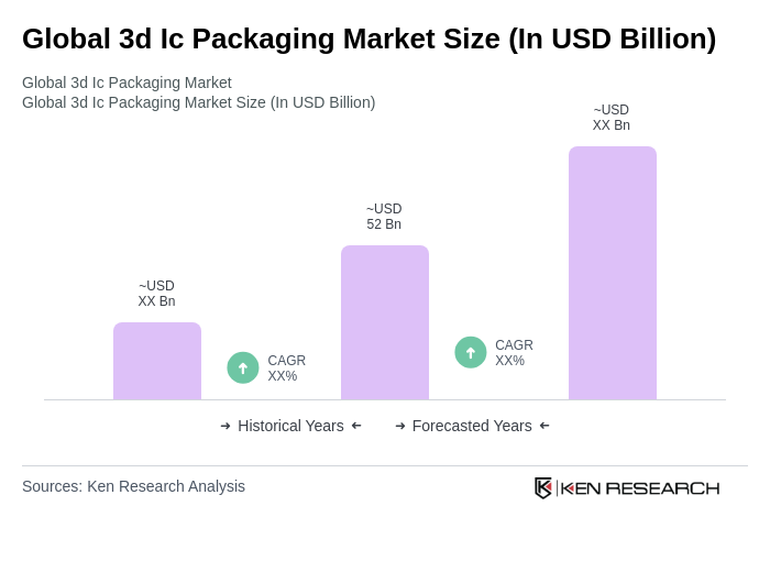
  • The Global 3D IC Packaging Market is valued at approximately USD 58–61 billion, based on a five-year analysis of authoritative industry sources and current-market rollups that combine 3D IC and 2.5D IC packaging revenues. This valuation aligns with recent industry estimates that place the combined 3D IC and 2.5D IC packaging market near the low-sixties in USD billions and reflects strong demand from AI/HPC, HBM, and advanced logic integration .
  • Key players in this market include countries like the United States, South Korea, and Taiwan, which dominate due to their strong semiconductor manufacturing capabilities and technological advancements. These regions host leading foundries, IDMs, and OSATs, including TSMC, Samsung, SK hynix, Micron, Intel, ASE, and Amkor, underpinning leadership in 2.5D/3D integration, HBM, CoWoS/SoIC, and hybrid bonding .
  • In 2023, the U.S. government implemented regulations to promote advanced semiconductor manufacturing, including 3D IC packaging technologies. This initiative includes a funding program of USD 52 billion under the CHIPS and Science Act to enhance domestic production capabilities and strengthen supply-chain resilience, supporting advanced packaging capacity expansions in the U.S. .
Global 3d Ic Packaging Market Size

Global 3D IC Packaging Market Segmentation

By Type:The 3D IC packaging market can be segmented into various types, including Through-Silicon Via (TSV) 3D Stacked Die, 2.5D Interposer-Based Packaging, Fan-Out Wafer-Level Packaging (FO-WLP/3D Fan-Out), Hybrid Bonding/Direct Bond Interconnect (DBI) 3D, System-in-Package (SiP) and Heterogeneous Integration, and Others (e.g., Package-on-Package, CoWoS/SoIC variants). Among these, the Through-Silicon Via (TSV) 3D Stacked Die is currently the leading subsegment due to its ability to provide high-density interconnections and improved performance for high-performance computing applications. The demand for TSV technology is driven by the increasing need for efficient thermal management, bandwidth scaling for HBM/AI accelerators, and power efficiency in advanced electronic devices .
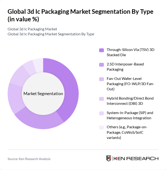
Global 3d Ic Packaging Market segmentation by Type.

By End-User:The end-user segmentation of the 3D IC packaging market includes Consumer Electronics, Automotive and Mobility, Telecommunications and 5G Infrastructure, Industrial and IoT, Data Center and Cloud/HPC, Healthcare and Medical Devices, and Aerospace & Defense. The Consumer Electronics segment remains significant due to smartphones, tablets, image sensors, and wearables; however, rapid adoption in Data Center and Cloud/HPC is accelerating with AI accelerators and HBM-enabled GPUs driving 2.5D/3D packaging uptake. IoT proliferation and 5G infrastructure also contribute to demand for miniaturization and higher bandwidth packaging .
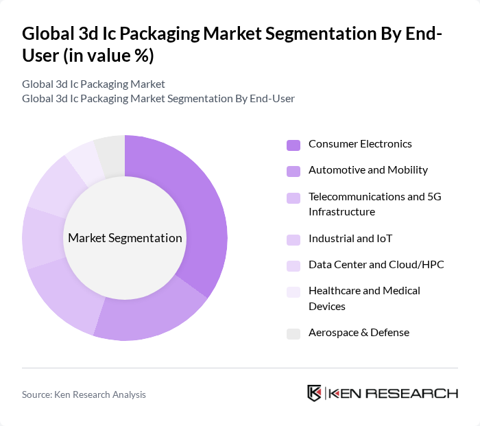
Global 3d Ic Packaging Market segmentation by End-User.

Global 3D IC Packaging Market Competitive Landscape

The Global 3D IC Packaging Market is characterized by a dynamic mix of regional and international players. Leading participants such as Taiwan Semiconductor Manufacturing Company Limited (TSMC), Samsung Electronics Co., Ltd., Intel Corporation, Micron Technology, Inc., SK hynix Inc., ASE Technology Holding Co., Ltd. (ASE Group), Amkor Technology, Inc., Advanced Micro Devices, Inc. (for 3D chiplet/3D V-Cache integration), Taiwan Union Technology Corporation (TUC), and Ibiden Co., Ltd. (advanced substrates), Shinko Electric Industries Co., Ltd., United Microelectronics Corporation (UMC), Powertech Technology Inc. (PTI), Jiangsu Changjiang Electronics Technology Co., Ltd. (JCET Group), STATS ChipPAC Pte. Ltd. (a JCET company), ASE-Siliconware Precision Industries Co., Ltd. (SPIL) contribute to innovation, geographic expansion, and service delivery in this space .

Taiwan Semiconductor Manufacturing Company Limited (TSMC)

1987

Hsinchu, Taiwan

Samsung Electronics Co., Ltd.

1969

Suwon, South Korea

Intel Corporation

1968

Santa Clara, California, USA

Micron Technology, Inc.

1978

Boise, Idaho, USA

SK hynix Inc.

1983

Icheon, South Korea

Company

Establishment Year

Headquarters

Segment Focus (Foundry, IDM, OSAT, Materials, EDA)

3D/2.5D Packaging Revenue (latest fiscal year, USD)

CAGR of Advanced Packaging Revenue (3–5 years)

Capacity Indicators (wafer starts/month; HBM/CoWoS/SoIC capacity)

Customer Concentration (top-3 revenue share)

Technology Readiness (TSV, hybrid bonding, 2.5D interposer, fan-out)

Global 3d Ic Packaging Market Industry Analysis

Growth Drivers

  • Increasing Demand for Miniaturization in Electronics:The global electronics market is projected to reach $1.5 trillion in future, driven by consumer preferences for smaller, more efficient devices. This trend is particularly evident in smartphones, which are expected to see an increase in demand for compact components. The miniaturization trend is pushing manufacturers to adopt 3D IC packaging solutions, which can significantly reduce the footprint of electronic devices while enhancing performance and functionality.
  • Advancements in Semiconductor Technology:The semiconductor industry is expected to invest over $200 billion in research and development in future, focusing on innovative technologies such as 3D integration. These advancements enable higher performance and lower power consumption, making 3D IC packaging an attractive option for manufacturers. As semiconductor technology evolves, the demand for advanced packaging solutions that can accommodate complex chip designs is anticipated to grow, further driving market expansion.
  • Rising Adoption of IoT Devices:The Internet of Things (IoT) market is projected to grow to $1.1 trillion in future, with billions of connected devices requiring efficient packaging solutions. 3D IC packaging is essential for IoT devices, as it allows for the integration of multiple functionalities in a compact form factor. This trend is expected to accelerate the adoption of 3D IC technologies, as manufacturers seek to meet the demands of a rapidly expanding IoT ecosystem.

Market Challenges

  • High Manufacturing Costs:The production of 3D IC packaging involves complex processes and advanced materials, leading to manufacturing costs that can exceed $100 million for new facilities. This high capital investment can deter smaller companies from entering the market, limiting competition and innovation. As a result, the overall growth of the 3D IC packaging market may be hindered by these financial barriers, particularly in regions with less access to funding.
  • Complexity in Design and Integration:The design and integration of 3D IC packaging require specialized knowledge and expertise, which can complicate the development process. With an estimated shortage of over 1 million skilled professionals in the semiconductor industry in future, companies may struggle to find qualified personnel to manage these complex projects. This skills gap can lead to delays in product development and increased costs, posing a significant challenge to market growth.

Global 3d Ic Packaging Market Future Outlook

The future of the 3D IC packaging market appears promising, driven by technological advancements and increasing demand for compact electronic solutions. As manufacturers continue to innovate, the integration of AI and machine learning in production processes is expected to enhance efficiency and reduce costs. Additionally, the growing emphasis on sustainability will likely lead to the development of eco-friendly packaging materials, further shaping the market landscape and attracting investment in new technologies.

Market Opportunities

  • Expansion in Emerging Markets:Emerging markets, particularly in Asia-Pacific, are expected to see a surge in demand for 3D IC packaging solutions, driven by rapid urbanization and increasing disposable incomes. With a projected growth rate of 8% in the electronics sector in these regions, companies can capitalize on this opportunity to expand their market presence and cater to the growing consumer base.
  • Development of New Materials:The ongoing research into advanced materials for 3D IC packaging presents significant opportunities for innovation. With an estimated $15 billion allocated for material science research in future, companies that invest in developing new, high-performance materials can differentiate themselves in the market, enhancing product offerings and attracting new customers.

Scope of the Report

SegmentSub-Segments
By Type

Through-Silicon Via (TSV) 3D Stacked Die

D Interposer-Based Packaging

Fan-Out Wafer-Level Packaging (FO-WLP/3D Fan-Out)

Hybrid Bonding/Direct Bond Interconnect (DBI) 3D

System-in-Package (SiP) and Heterogeneous Integration

Others (e.g., Package-on-Package, CoWoS/SoIC variants)

By End-User

Consumer Electronics

Automotive and Mobility

Telecommunications and 5G Infrastructure

Industrial and IoT

Data Center and Cloud/HPC

Healthcare and Medical Devices

Aerospace & Defense

By Application

High-Performance Computing (AI/Accelerators)

Mobile and Wearables

Networking and Edge Computing

Memory (HBM/3D NAND) and Storage

Imaging Sensors and MEMS

Advanced Driver-Assistance Systems (ADAS) and EV Power Electronics

Others

By Material

Silicon (wafers, interposers)

Organic Substrates and Build-Up laminates

Glass Interposers

Advanced Dielectrics, Underfill, and Mold Compounds

Solder Balls, Micro-bumps, and Cu Pillars

Thermal Interface Materials

Others

By Distribution Channel

Direct Manufacturer Engagement (OSAT/Foundry)

Authorized Distributors and Design Partners

Turnkey/EMS and ODM Channels

Online and Platform-Based Procurement

Others

By Region

North America

Europe

Asia-Pacific

Latin America

Middle East & Africa

By Price Range

Entry-Level (Cost-Optimized)

Mid-Range (Performance/Cost Balance)

Premium (High-Performance/Advanced Node)

Custom/Specialized

Key Target Audience

Investors and Venture Capitalist Firms

Government and Regulatory Bodies (e.g., U.S. Department of Commerce, European Commission)

Manufacturers and Producers

Distributors and Retailers

Technology Providers

Industry Associations (e.g., SEMI, IPC)

Financial Institutions

Original Equipment Manufacturers (OEMs)

Players Mentioned in the Report:

Taiwan Semiconductor Manufacturing Company Limited (TSMC)

Samsung Electronics Co., Ltd.

Intel Corporation

Micron Technology, Inc.

SK hynix Inc.

ASE Technology Holding Co., Ltd. (ASE Group)

Amkor Technology, Inc.

Advanced Micro Devices, Inc. (for 3D chiplet/3D V-Cache integration)

Taiwan Union Technology Corporation (TUC) and Ibiden Co., Ltd. (advanced substrates)

Shinko Electric Industries Co., Ltd.

United Microelectronics Corporation (UMC)

Powertech Technology Inc. (PTI)

Jiangsu Changjiang Electronics Technology Co., Ltd. (JCET Group)

STATS ChipPAC Pte. Ltd. (a JCET company)

ASE-Siliconware Precision Industries Co., Ltd. (SPIL)

Table of Contents

Market Assessment Phase

1. Executive Summary and Approach


2. Global 3d Ic Packaging Market Overview

2.1 Key Insights and Strategic Recommendations

2.2 Global 3d Ic Packaging Market Overview

2.3 Definition and Scope

2.4 Evolution of Market Ecosystem

2.5 Timeline of Key Regulatory Milestones

2.6 Value Chain & Stakeholder Mapping

2.7 Business Cycle Analysis

2.8 Policy & Incentive Landscape


3. Global 3d Ic Packaging Market Analysis

3.1 Growth Drivers

3.1.1 Increasing demand for miniaturization in electronics
3.1.2 Advancements in semiconductor technology
3.1.3 Rising adoption of IoT devices
3.1.4 Growth in consumer electronics market

3.2 Market Challenges

3.2.1 High manufacturing costs
3.2.2 Complexity in design and integration
3.2.3 Limited availability of skilled workforce
3.2.4 Stringent regulatory requirements

3.3 Market Opportunities

3.3.1 Expansion in emerging markets
3.3.2 Development of new materials
3.3.3 Collaborations and partnerships
3.3.4 Increasing investment in R&D

3.4 Market Trends

3.4.1 Shift towards 3D integration technologies
3.4.2 Growing focus on sustainability
3.4.3 Rise of AI and machine learning in manufacturing
3.4.4 Increasing customization in packaging solutions

3.5 Government Regulation

3.5.1 Environmental compliance standards
3.5.2 Safety regulations for electronic components
3.5.3 Trade policies affecting semiconductor imports
3.5.4 Incentives for R&D in packaging technologies

4. SWOT Analysis


5. Stakeholder Analysis


6. Porter's Five Forces Analysis


7. Global 3d Ic Packaging Market Market Size, 2019-2024

7.1 By Value

7.2 By Volume

7.3 By Average Selling Price


8. Global 3d Ic Packaging Market Segmentation

8.1 By Type

8.1.1 Through-Silicon Via (TSV) 3D Stacked Die
8.1.2 2.5D Interposer-Based Packaging
8.1.3 Fan-Out Wafer-Level Packaging (FO-WLP/3D Fan-Out)
8.1.4 Hybrid Bonding/Direct Bond Interconnect (DBI) 3D
8.1.5 System-in-Package (SiP) and Heterogeneous Integration
8.1.6 Others (e.g., Package-on-Package, CoWoS/SoIC variants)

8.2 By End-User

8.2.1 Consumer Electronics
8.2.2 Automotive and Mobility
8.2.3 Telecommunications and 5G Infrastructure
8.2.4 Industrial and IoT
8.2.5 Data Center and Cloud/HPC
8.2.6 Healthcare and Medical Devices
8.2.7 Aerospace & Defense

8.3 By Application

8.3.1 High-Performance Computing (AI/Accelerators)
8.3.2 Mobile and Wearables
8.3.3 Networking and Edge Computing
8.3.4 Memory (HBM/3D NAND) and Storage
8.3.5 Imaging Sensors and MEMS
8.3.6 Advanced Driver-Assistance Systems (ADAS) and EV Power Electronics
8.3.7 Others

8.4 By Material

8.4.1 Silicon (wafers, interposers)
8.4.2 Organic Substrates and Build-Up laminates
8.4.3 Glass Interposers
8.4.4 Advanced Dielectrics, Underfill, and Mold Compounds
8.4.5 Solder Balls, Micro-bumps, and Cu Pillars
8.4.6 Thermal Interface Materials
8.4.7 Others

8.5 By Distribution Channel

8.5.1 Direct Manufacturer Engagement (OSAT/Foundry)
8.5.2 Authorized Distributors and Design Partners
8.5.3 Turnkey/EMS and ODM Channels
8.5.4 Online and Platform-Based Procurement
8.5.5 Others

8.6 By Region

8.6.1 North America
8.6.2 Europe
8.6.3 Asia-Pacific
8.6.4 Latin America
8.6.5 Middle East & Africa

8.7 By Price Range

8.7.1 Entry-Level (Cost-Optimized)
8.7.2 Mid-Range (Performance/Cost Balance)
8.7.3 Premium (High-Performance/Advanced Node)
8.7.4 Custom/Specialized

9. Global 3d Ic Packaging Market Competitive Analysis

9.1 Market Share of Key Players

9.2 Cross Comparison of Key Players

9.2.1 Company Name
9.2.2 Segment Focus (Foundry, IDM, OSAT, Materials, EDA)
9.2.3 3D/2.5D Packaging Revenue (latest fiscal year, USD)
9.2.4 CAGR of Advanced Packaging Revenue (3–5 years)
9.2.5 Capacity Indicators (wafer starts/month; HBM/CoWoS/SoIC capacity)
9.2.6 Customer Concentration (top-3 revenue share)
9.2.7 Technology Readiness (TSV, hybrid bonding, 2.5D interposer, fan-out)
9.2.8 Time-to-Ramp for New Nodes/Packages
9.2.9 Yield and Line Utilization (%)
9.2.10 Supply Chain Resilience (multi-site, geographic diversity)
9.2.11 CapEx Intensity (% of revenue)
9.2.12 Patent Portfolio Strength (3D/heterogeneous integration patents)
9.2.13 Design Ecosystem Enablement (chiplet/IP, EDA co-optimization)
9.2.14 ESG and Energy Efficiency Metrics

9.3 SWOT Analysis of Top Players

9.4 Pricing Analysis

9.5 Detailed Profile of Major Companies

9.5.1 Taiwan Semiconductor Manufacturing Company Limited (TSMC)
9.5.2 Samsung Electronics Co., Ltd.
9.5.3 Intel Corporation
9.5.4 Micron Technology, Inc.
9.5.5 SK hynix Inc.
9.5.6 ASE Technology Holding Co., Ltd. (ASE Group)
9.5.7 Amkor Technology, Inc.
9.5.8 Advanced Micro Devices, Inc. (for 3D chiplet/3D V-Cache integration)
9.5.9 Taiwan Union Technology Corporation (TUC) and Ibiden Co., Ltd. (advanced substrates)
9.5.10 Shinko Electric Industries Co., Ltd.
9.5.11 United Microelectronics Corporation (UMC)
9.5.12 Powertech Technology Inc. (PTI)
9.5.13 Jiangsu Changjiang Electronics Technology Co., Ltd. (JCET Group)
9.5.14 STATS ChipPAC Pte. Ltd. (a JCET company)
9.5.15 ASE-Siliconware Precision Industries Co., Ltd. (SPIL)

10. Global 3d Ic Packaging Market End-User Analysis

10.1 Procurement Behavior of Key Ministries

10.1.1 Government contracts for electronics
10.1.2 Budget allocation for technology upgrades
10.1.3 Compliance with procurement regulations

10.2 Corporate Spend on Infrastructure & Energy

10.2.1 Investment in semiconductor facilities
10.2.2 Funding for R&D in packaging technologies
10.2.3 Expenditure on sustainable practices

10.3 Pain Point Analysis by End-User Category

10.3.1 Supply chain disruptions
10.3.2 Quality control issues
10.3.3 Cost management challenges

10.4 User Readiness for Adoption

10.4.1 Awareness of 3D IC benefits
10.4.2 Training and skill development needs
10.4.3 Infrastructure readiness

10.5 Post-Deployment ROI and Use Case Expansion

10.5.1 Measurement of performance improvements
10.5.2 Scalability of solutions
10.5.3 Long-term cost savings

11. Global 3d Ic Packaging Market Future Size, 2025-2030

11.1 By Value

11.2 By Volume

11.3 By Average Selling Price


Go-To-Market Strategy Phase

1. Whitespace Analysis + Business Model Canvas

1.1 Market gaps and opportunities

1.2 Value proposition development

1.3 Revenue model exploration

1.4 Customer segmentation

1.5 Key partnerships

1.6 Cost structure analysis

1.7 Competitive landscape


2. Marketing and Positioning Recommendations

2.1 Branding strategies

2.2 Product USPs

2.3 Target audience identification

2.4 Communication strategies

2.5 Digital marketing initiatives


3. Distribution Plan

3.1 Urban retail strategies

3.2 Rural NGO tie-ups

3.3 E-commerce integration

3.4 Logistics and supply chain management


4. Channel & Pricing Gaps

4.1 Underserved routes

4.2 Pricing bands analysis

4.3 Competitor pricing strategies

4.4 Customer willingness to pay


5. Unmet Demand & Latent Needs

5.1 Category gaps

5.2 Consumer segments

5.3 Product development opportunities


6. Customer Relationship

6.1 Loyalty programs

6.2 After-sales service

6.3 Customer feedback mechanisms


7. Value Proposition

7.1 Sustainability initiatives

7.2 Integrated supply chains

7.3 Competitive advantages


8. Key Activities

8.1 Regulatory compliance

8.2 Branding efforts

8.3 Distribution setup


9. Entry Strategy Evaluation

9.1 Domestic Market Entry Strategy

9.1.1 Product mix considerations
9.1.2 Pricing band analysis
9.1.3 Packaging strategies

9.2 Export Entry Strategy

9.2.1 Target countries identification
9.2.2 Compliance roadmap development

10. Entry Mode Assessment

10.1 Joint Ventures

10.2 Greenfield investments

10.3 Mergers & Acquisitions

10.4 Distributor Model


11. Capital and Timeline Estimation

11.1 Capital requirements

11.2 Timelines for market entry


12. Control vs Risk Trade-Off

12.1 Ownership considerations

12.2 Partnerships evaluation


13. Profitability Outlook

13.1 Breakeven analysis

13.2 Long-term sustainability strategies


14. Potential Partner List

14.1 Distributors

14.2 Joint Ventures

14.3 Acquisition targets


15. Execution Roadmap

15.1 Phased Plan for Market Entry

15.1.1 Market Setup
15.1.2 Market Entry
15.1.3 Growth Acceleration
15.1.4 Scale & Stabilize

15.2 Key Activities and Milestones

15.2.1 Activity timelines
15.2.2 Milestone tracking

Research Methodology

ApproachModellingSample

Phase 1: Approach1

Desk Research

  • Industry reports from semiconductor associations and packaging technology journals
  • Market analysis from trade publications focusing on 3D IC packaging trends
  • Statistical data from government and industry databases on semiconductor production

Primary Research

  • Interviews with R&D heads at leading semiconductor manufacturers
  • Surveys with supply chain experts in the electronics packaging sector
  • Field interviews with engineers specializing in 3D IC design and packaging

Validation & Triangulation

  • Cross-validation of findings through multiple industry reports and white papers
  • Triangulation of data from primary interviews and secondary sources
  • Sanity checks conducted through expert panels comprising industry veterans

Phase 2: Market Size Estimation1

Top-down Assessment

  • Analysis of global semiconductor market size and growth rates
  • Segmentation of the 3D IC packaging market by application and geography
  • Incorporation of trends in consumer electronics and automotive sectors

Bottom-up Modeling

  • Volume estimates based on production capacities of key manufacturers
  • Cost analysis derived from pricing models of 3D IC packaging solutions
  • Estimation of market share based on sales data from leading firms

Forecasting & Scenario Analysis

  • Multi-variable regression analysis incorporating technological advancements and market demand
  • Scenario planning based on potential regulatory changes and market disruptions
  • Development of baseline, optimistic, and pessimistic forecasts through 2030

Phase 3: CATI Sample Composition1

Scope Item/SegmentSample SizeTarget Respondent Profiles
Consumer Electronics Manufacturers110Product Development Managers, Supply Chain Analysts
Automotive Electronics Suppliers85Engineering Managers, Procurement Specialists
Telecommunications Equipment Providers75Technical Directors, Operations Managers
Medical Device Manufacturers60Quality Assurance Managers, Regulatory Affairs Specialists
Research Institutions and Universities50Academic Researchers, Industry Collaborators

Frequently Asked Questions

What is the current value of the Global 3D IC Packaging Market?

The Global 3D IC Packaging Market is valued at approximately USD 5861 billion, reflecting strong demand driven by sectors such as AI, high-performance computing (HPC), and advanced logic integration, according to recent industry analyses.

Which countries are leading in the 3D IC Packaging Market?

What are the key drivers of growth in the 3D IC Packaging Market?

What challenges does the 3D IC Packaging Market face?

Other Regional/Country Reports

Indonesia Global 3d Ic Packaging Market

Malaysia Global 3d Ic Packaging Market

KSA Global 3d Ic Packaging Market

APAC Global 3d Ic Packaging Market

SEA Global 3d Ic Packaging Market

Vietnam Global 3d Ic Packaging Market

Why Buy From Us?

Refine Robust Result (RRR) Framework

What makes us stand out is that our consultants follow Robust, Refine and Result (RRR) methodology. Robust for clear definitions, approaches and sanity checking, Refine for differentiating respondents' facts and opinions, and Result for presenting data with story.

Our Reach Is Unmatched

We have set a benchmark in the industry by offering our clients with syndicated and customized market research reports featuring coverage of entire market as well as meticulous research and analyst insights.

Shifting the Research Paradigm

While we don't replace traditional research, we flip the method upside down. Our dual approach of Top Bottom & Bottom Top ensures quality deliverable by not just verifying company fundamentals but also looking at the sector and macroeconomic factors.

More Insights-Better Decisions

With one step in the future, our research team constantly tries to show you the bigger picture. We help with some of the tough questions you may encounter along the way: How is the industry positioned? Best marketing channel? KPI's of competitors? By aligning every element, we help maximize success.

Transparency and Trust

Our report gives you instant access to the answers and sources that other companies might choose to hide. We elaborate each steps of research methodology we have used and showcase you the sample size to earn your trust.

Round the Clock Support

If you need any support, we are here! We pride ourselves on universe strength, data quality, and quick, friendly, and professional service.

Why Clients Choose Us?

400000+
Reports in repository
150+
Consulting projects a year
100+
Analysts
8000+
Client Queries in 2022