About the Report
Base Year 2024Global Extreme Ultraviolet Lithography Market Overview
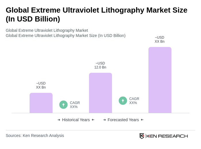
- The Global Extreme Ultraviolet Lithography Market is valued at USD 12.0 billion, based on a five-year historical analysis. This growth is primarily driven by the increasing demand for advanced semiconductor manufacturing technologies, particularly for sub-7nm node production, which require high-resolution lithography solutions. The rise in consumer electronics, proliferation of IoT devices, and the rapid adoption of AI and 5G technologies have further fueled the need for smaller, more efficient chips, thereby boosting the market for extreme ultraviolet lithography .
- Key players in this market include countries such as the United States, South Korea, and Taiwan, which dominate due to their strong semiconductor manufacturing capabilities and technological advancements. The presence of major semiconductor foundries and integrated device manufacturers in these regions has created a robust ecosystem that supports the growth of extreme ultraviolet lithography technologies .
- In 2023, the U.S. government implemented regulations aimed at enhancing semiconductor manufacturing capabilities, including a funding initiative of USD 52 billion to support research and development in advanced lithography technologies. This initiative is designed to strengthen the domestic semiconductor supply chain and reduce reliance on foreign technologies .

Global Extreme Ultraviolet Lithography Market Segmentation
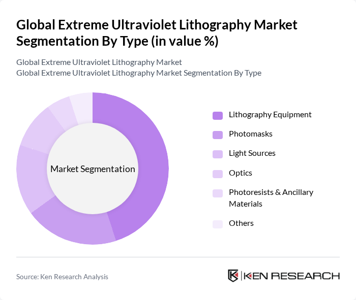
By Type:The market can be segmented into lithography equipment, photomasks, light sources, optics, photoresists & ancillary materials, and others. Among these, lithography equipment is the most significant segment, driven by the increasing demand for high-precision manufacturing in the semiconductor industry. Advancements in photomask technology and light sources also contribute to overall growth, as they are essential components in the lithography process. The adoption of high-NA (numerical aperture) EUV systems and improvements in mask and light source reliability are key trends shaping this segment .

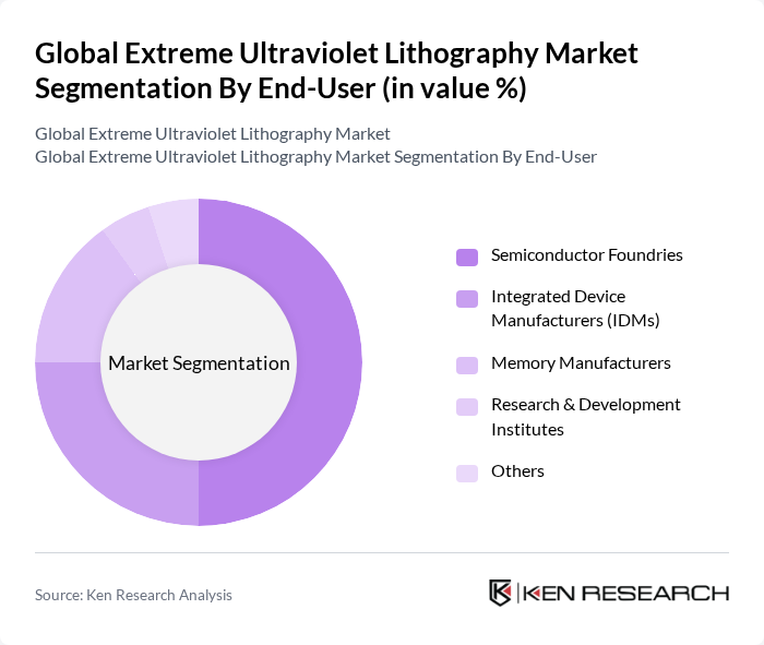
By End-User:The end-user segmentation includes semiconductor foundries, integrated device manufacturers (IDMs), memory manufacturers, research & development institutes, and others. Semiconductor foundries are the leading segment, as they require advanced lithography solutions for producing high-performance chips. The increasing demand for memory and logic devices further drives the growth of this segment, while IDMs and research institutes also contribute significantly to the market. The adoption of EUV lithography by leading foundries such as TSMC, Samsung, and Intel is a major growth driver in this segment .

Global Extreme Ultraviolet Lithography Market Competitive Landscape
The Global Extreme Ultraviolet Lithography Market is characterized by a dynamic mix of regional and international players. Leading participants such as ASML Holding N.V., Nikon Corporation, Canon Inc., Intel Corporation, Samsung Electronics Co., Ltd., Taiwan Semiconductor Manufacturing Company Limited (TSMC), GlobalFoundries Inc., Micron Technology, Inc., Advanced Micro Devices, Inc. (AMD), Texas Instruments Incorporated, STMicroelectronics N.V., Infineon Technologies AG, Broadcom Inc., NXP Semiconductors N.V., Renesas Electronics Corporation, SK hynix Inc., Lam Research Corporation, KLA Corporation, Carl Zeiss AG, Tokyo Electron Limited contribute to innovation, geographic expansion, and service delivery in this space.
Global Extreme Ultraviolet Lithography Market Industry Analysis
Growth Drivers
- Increasing Demand for Advanced Semiconductor Manufacturing:The global semiconductor market is projected to reach $1 trillion in future, driven by the demand for advanced chips in various applications. In future, the semiconductor industry is expected to invest approximately $200 billion in manufacturing capabilities, with a significant portion allocated to extreme ultraviolet lithography (EUV) technology. This surge in investment is primarily fueled by the need for smaller, more efficient chips that can support emerging technologies like AI and 5G, thereby enhancing the EUV market's growth prospects.
- Technological Advancements in Lithography Equipment:The EUV lithography equipment market is witnessing rapid technological advancements, with companies like ASML leading the charge. In future, ASML is expected to deliver over 50 EUV machines, each costing around $150 million. These machines enable the production of chips with features as small as 3 nanometers, significantly enhancing performance and efficiency. The continuous innovation in lithography technology is crucial for meeting the increasing demands of semiconductor manufacturers, thereby driving market growth.
- Rising Investment in Research and Development:Global investment in semiconductor R&D is projected to exceed $40 billion in future, reflecting a robust commitment to innovation. Major players, including Intel and TSMC, are allocating substantial budgets to develop next-generation lithography technologies. This investment is essential for advancing EUV capabilities, improving yield rates, and reducing production costs. As companies strive to maintain competitive advantages, the focus on R&D will significantly bolster the EUV lithography market's growth trajectory.
Market Challenges
- High Initial Investment Costs:The high capital expenditure associated with EUV lithography systems poses a significant barrier to entry for many semiconductor manufacturers. The cost of a single EUV machine can exceed $150 million, which is a substantial investment for companies, especially smaller players. In future, it is estimated that only a handful of manufacturers will be able to afford these systems, limiting market participation and potentially stifling innovation in the sector.
- Complexity of Technology Integration:Integrating EUV lithography into existing semiconductor manufacturing processes presents considerable challenges. The complexity of the technology requires specialized knowledge and skills, which are currently in short supply. In future, it is anticipated that only 30% of semiconductor manufacturers will successfully implement EUV technology into their production lines. This complexity can lead to delays in production and increased operational costs, hindering overall market growth.
Global Extreme Ultraviolet Lithography Market Future Outlook
The future of the EUV lithography market appears promising, driven by the increasing demand for advanced semiconductor technologies and the ongoing push for miniaturization. As manufacturers continue to invest in R&D and technological advancements, the integration of EUV systems is expected to become more streamlined. Additionally, the expansion of 5G networks and the rise of AI and IoT applications will further fuel the need for high-performance chips, creating a favorable environment for EUV lithography growth in the coming years.
Market Opportunities
- Growth in 5G Technology Deployment:The global rollout of 5G technology is anticipated to create significant demand for advanced semiconductor solutions. In future, the number of 5G connections is expected to reach 1.5 billion, necessitating the production of high-performance chips. This demand presents a substantial opportunity for EUV lithography, as manufacturers seek to develop smaller, more efficient components to support 5G infrastructure.
- Increasing Adoption of AI and IoT Devices:The proliferation of AI and IoT devices is driving the need for advanced semiconductor manufacturing. In future, the global AI market is projected to reach $500 billion, while IoT devices are expected to exceed 30 billion units. This growth will require cutting-edge chips, creating a significant opportunity for EUV lithography to meet the demands of these rapidly evolving technologies.
Scope of the Report
| Segment | Sub-Segments |
|---|---|
| By Type | Lithography Equipment Photomasks Light Sources Optics Photoresists & Ancillary Materials Others |
| By End-User | Semiconductor Foundries Integrated Device Manufacturers (IDMs) Memory Manufacturers Research & Development Institutes Others |
| By Application | Logic IC Manufacturing Memory IC Manufacturing Advanced Packaging MEMS & Sensors Nanotechnology Others |
| By Component | Hardware Software Services |
| By Sales Channel | Direct Sales Distributors Online Sales |
| By Distribution Mode | Offline Distribution Online Distribution |
| By Price Range | Premium Mid-Range Budget |
Key Target Audience
Investors and Venture Capitalist Firms
Government and Regulatory Bodies (e.g., U.S. Department of Commerce, European Commission)
Manufacturers and Producers of Semiconductor Equipment
Distributors and Suppliers of Photolithography Materials
Technology Providers in Semiconductor Fabrication
Industry Associations (e.g., Semiconductor Industry Association)
Financial Institutions and Investment Banks
Research and Development Organizations in Nanotechnology
Players Mentioned in the Report:
ASML Holding N.V.
Nikon Corporation
Canon Inc.
Intel Corporation
Samsung Electronics Co., Ltd.
Taiwan Semiconductor Manufacturing Company Limited (TSMC)
GlobalFoundries Inc.
Micron Technology, Inc.
Advanced Micro Devices, Inc. (AMD)
Texas Instruments Incorporated
STMicroelectronics N.V.
Infineon Technologies AG
Broadcom Inc.
NXP Semiconductors N.V.
Renesas Electronics Corporation
SK hynix Inc.
Lam Research Corporation
KLA Corporation
Carl Zeiss AG
Tokyo Electron Limited
Table of Contents
Market Assessment Phase
1. Executive Summary and Approach
2. Global Extreme Ultraviolet Lithography Market Overview
2.1 Key Insights and Strategic Recommendations
2.2 Global Extreme Ultraviolet Lithography Market Overview
2.3 Definition and Scope
2.4 Evolution of Market Ecosystem
2.5 Timeline of Key Regulatory Milestones
2.6 Value Chain & Stakeholder Mapping
2.7 Business Cycle Analysis
2.8 Policy & Incentive Landscape
3. Global Extreme Ultraviolet Lithography Market Analysis
3.1 Growth Drivers
3.1.1 Increasing Demand for Advanced Semiconductor Manufacturing
3.1.2 Technological Advancements in Lithography Equipment
3.1.3 Rising Investment in Research and Development
3.1.4 Expansion of Electronics and Consumer Goods Markets
3.2 Market Challenges
3.2.1 High Initial Investment Costs
3.2.2 Complexity of Technology Integration
3.2.3 Supply Chain Disruptions
3.2.4 Regulatory Compliance Issues
3.3 Market Opportunities
3.3.1 Growth in 5G Technology Deployment
3.3.2 Increasing Adoption of AI and IoT Devices
3.3.3 Expansion into Emerging Markets
3.3.4 Collaborations and Partnerships for Innovation
3.4 Market Trends
3.4.1 Shift Towards Miniaturization of Electronic Components
3.4.2 Adoption of Sustainable Manufacturing Practices
3.4.3 Integration of AI in Lithography Processes
3.4.4 Focus on Customization and Flexibility in Production
3.5 Government Regulation
3.5.1 Environmental Compliance Standards
3.5.2 Export Control Regulations
3.5.3 Safety and Health Regulations
3.5.4 Incentives for Research and Development
4. SWOT Analysis
5. Stakeholder Analysis
6. Porter's Five Forces Analysis
7. Global Extreme Ultraviolet Lithography Market Market Size, 2019-2024
7.1 By Value
7.2 By Volume
7.3 By Average Selling Price
8. Global Extreme Ultraviolet Lithography Market Segmentation
8.1 By Type
8.1.1 Lithography Equipment
8.1.2 Photomasks
8.1.3 Light Sources
8.1.4 Optics
8.1.5 Photoresists & Ancillary Materials
8.1.6 Others
8.2 By End-User
8.2.1 Semiconductor Foundries
8.2.2 Integrated Device Manufacturers (IDMs)
8.2.3 Memory Manufacturers
8.2.4 Research & Development Institutes
8.2.5 Others
8.3 By Application
8.3.1 Logic IC Manufacturing
8.3.2 Memory IC Manufacturing
8.3.3 Advanced Packaging
8.3.4 MEMS & Sensors
8.3.5 Nanotechnology
8.3.6 Others
8.4 By Component
8.4.1 Hardware
8.4.2 Software
8.4.3 Services
8.5 By Sales Channel
8.5.1 Direct Sales
8.5.2 Distributors
8.5.3 Online Sales
8.6 By Distribution Mode
8.6.1 Offline Distribution
8.6.2 Online Distribution
8.7 By Price Range
8.7.1 Premium
8.7.2 Mid-Range
8.7.3 Budget
9. Global Extreme Ultraviolet Lithography Market Competitive Analysis
9.1 Market Share of Key Players
9.2 Cross Comparison of Key Players
9.2.1 Company Name
9.2.2 Company Type (Equipment Supplier, Foundry, IDM, Memory Manufacturer, etc.)
9.2.3 Revenue (USD, Latest Fiscal Year)
9.2.4 EUV Lithography Market Share (%)
9.2.5 Installed Base of EUV Systems
9.2.6 R&D Expenditure (% of Revenue)
9.2.7 Number of Patents Related to EUV
9.2.8 Average Throughput (Wafers per Hour)
9.2.9 Yield Rate (%)
9.2.10 Customer Base (Number of Major Clients)
9.2.11 Geographic Presence (Regions Served)
9.2.12 Supply Chain Reliability Index
9.2.13 Strategic Partnerships & Alliances
9.3 SWOT Analysis of Top Players
9.4 Pricing Analysis
9.5 Detailed Profile of Major Companies
9.5.1 ASML Holding N.V.
9.5.2 Nikon Corporation
9.5.3 Canon Inc.
9.5.4 Intel Corporation
9.5.5 Samsung Electronics Co., Ltd.
9.5.6 Taiwan Semiconductor Manufacturing Company Limited (TSMC)
9.5.7 GlobalFoundries Inc.
9.5.8 Micron Technology, Inc.
9.5.9 Advanced Micro Devices, Inc. (AMD)
9.5.10 Texas Instruments Incorporated
9.5.11 STMicroelectronics N.V.
9.5.12 Infineon Technologies AG
9.5.13 Broadcom Inc.
9.5.14 NXP Semiconductors N.V.
9.5.15 Renesas Electronics Corporation
9.5.16 SK hynix Inc.
9.5.17 Lam Research Corporation
9.5.18 KLA Corporation
9.5.19 Carl Zeiss AG
9.5.20 Tokyo Electron Limited
10. Global Extreme Ultraviolet Lithography Market End-User Analysis
10.1 Procurement Behavior of Key Ministries
10.1.1 Government Procurement Policies
10.1.2 Budget Allocation Trends
10.1.3 Decision-Making Processes
10.2 Corporate Spend on Infrastructure & Energy
10.2.1 Investment Trends in Semiconductor Infrastructure
10.2.2 Energy Consumption Patterns
10.2.3 Budgeting for R&D
10.3 Pain Point Analysis by End-User Category
10.3.1 Challenges in Technology Adoption
10.3.2 Cost Management Issues
10.3.3 Supply Chain Constraints
10.4 User Readiness for Adoption
10.4.1 Awareness of EUV Technology
10.4.2 Training and Skill Development Needs
10.4.3 Infrastructure Readiness
10.5 Post-Deployment ROI and Use Case Expansion
10.5.1 Measurement of ROI
10.5.2 Expansion into New Applications
10.5.3 Long-term Sustainability Considerations
11. Global Extreme Ultraviolet Lithography Market Future Size, 2025-2030
11.1 By Value
11.2 By Volume
11.3 By Average Selling Price
Go-To-Market Strategy Phase
1. Whitespace Analysis + Business Model Canvas
1.1 Market Gaps Identification
1.2 Business Model Development
2. Marketing and Positioning Recommendations
2.1 Branding Strategies
2.2 Product USPs
3. Distribution Plan
3.1 Urban Retail Strategies
3.2 Rural NGO Tie-ups
4. Channel & Pricing Gaps
4.1 Underserved Routes
4.2 Pricing Bands
5. Unmet Demand & Latent Needs
5.1 Category Gaps
5.2 Consumer Segments
6. Customer Relationship
6.1 Loyalty Programs
6.2 After-sales Service
7. Value Proposition
7.1 Sustainability
7.2 Integrated Supply Chains
8. Key Activities
8.1 Regulatory Compliance
8.2 Branding
8.3 Distribution Setup
9. Entry Strategy Evaluation
9.1 Domestic Market Entry Strategy
9.1.1 Product Mix
9.1.2 Pricing Band
9.1.3 Packaging
9.2 Export Entry Strategy
9.2.1 Target Countries
9.2.2 Compliance Roadmap
10. Entry Mode Assessment
10.1 Joint Ventures
10.2 Greenfield Investments
10.3 Mergers & Acquisitions
10.4 Distributor Model
11. Capital and Timeline Estimation
11.1 Capital Requirements
11.2 Timelines
12. Control vs Risk Trade-Off
12.1 Ownership vs Partnerships
13. Profitability Outlook
13.1 Breakeven Analysis
13.2 Long-term Sustainability
14. Potential Partner List
14.1 Distributors
14.2 Joint Ventures
14.3 Acquisition Targets
15. Execution Roadmap
15.1 Phased Plan for Market Entry
15.1.1 Market Setup
15.1.2 Market Entry
15.1.3 Growth Acceleration
15.1.4 Scale & Stabilize
15.2 Key Activities and Milestones
15.2.1 Activity Planning
15.2.2 Milestone Tracking
Research Methodology
Phase 1: Approach1
Desk Research
- Industry reports from semiconductor and photolithography associations
- Market analysis publications from leading research firms
- Technical papers and white papers on extreme ultraviolet lithography advancements
Primary Research
- Interviews with R&D heads at semiconductor manufacturing companies
- Surveys with equipment suppliers and technology providers in the EUV space
- Field interviews with process engineers and lithography specialists
Validation & Triangulation
- Cross-validation of market data through multiple industry sources
- Triangulation of findings from primary interviews and secondary data
- Sanity checks through expert panels comprising industry veterans
Phase 2: Market Size Estimation1
Top-down Assessment
- Analysis of global semiconductor market size and growth trends
- Segmentation by application areas such as consumer electronics, automotive, and telecommunications
- Incorporation of government initiatives promoting advanced manufacturing technologies
Bottom-up Modeling
- Volume estimates based on production capacities of leading semiconductor fabs
- Cost analysis of EUV lithography systems and their operational expenses
- Revenue projections based on unit sales and service contracts
Forecasting & Scenario Analysis
- Multi-variable regression analysis incorporating technological adoption rates
- Scenario modeling based on market demand fluctuations and supply chain disruptions
- Baseline, optimistic, and pessimistic forecasts through 2030
Phase 3: CATI Sample Composition1
| Scope Item/Segment | Sample Size | Target Respondent Profiles |
|---|---|---|
| Semiconductor Manufacturing | 100 | Manufacturing Engineers, Production Managers |
| Equipment Suppliers | 60 | Sales Directors, Product Managers |
| Research Institutions | 40 | Research Scientists, Lab Managers |
| End-user Industries | 50 | Product Development Managers, Procurement Officers |
| Regulatory Bodies | 40 | Policy Makers, Compliance Officers |
Frequently Asked Questions
What is the current value of the Global Extreme Ultraviolet Lithography Market?
The Global Extreme Ultraviolet Lithography Market is valued at approximately USD 12.0 billion, driven by the increasing demand for advanced semiconductor manufacturing technologies, particularly for sub-7nm node production, which requires high-resolution lithography solutions.