Global Gallium Arsenide Gaas Wafer Market

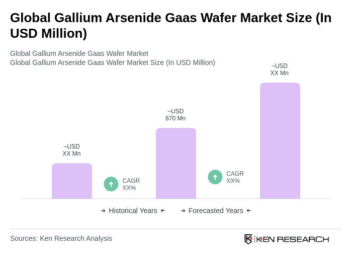
The Global Gallium Arsenide GaAs Wafer Market, valued at USD 670 million, is expanding due to demand for 5G, RF devices, solar cells, and LEDs, led by Asia-Pacific regions.

Region:Global

Author(s):Rebecca

Product Code:KRAC0317

Pages:99

Published On:August 2025
About the Report

Base Year 2024

Global Gallium Arsenide Gaas Wafer Market Overview

  • The Global Gallium Arsenide (GaAs) Wafer Market is valued at USD 670 million, based on a five-year historical analysis. This growth is primarily driven by the increasing demand for high-performance electronic devices, particularly in telecommunications and consumer electronics. The expansion of 5G infrastructure, rapid adoption of IoT devices, and rising applications in RF devices, solar cells, and LED technology have significantly contributed to the market's expansion, reflecting the growing trend towards advanced semiconductor materials .
  • Key players in this market include countries in Asia-Pacific, notably China, Japan, and South Korea, which dominate due to their strong manufacturing infrastructure, significant investments in research and development, and robust semiconductor supply chains. The United States and Germany also maintain prominent positions, supported by leading semiconductor companies and a high level of innovation .
  • In 2023, the U.S. government implemented regulations aimed at enhancing the domestic semiconductor supply chain, including a USD 52 billion investment to support semiconductor manufacturing and research. This initiative is designed to reduce reliance on foreign suppliers and bolster the U.S. position in the global semiconductor market, including GaAs wafers .
Global Gallium Arsenide Gaas Wafer Market Size

Global Gallium Arsenide Gaas Wafer Market Segmentation

By Type:The GaAs wafer market is segmented into Epitaxial Wafer, Substrate Wafer, Reclaimed Wafer, and Others. Among these, the Epitaxial Wafer segment leads due to its critical role in high-frequency and high-power applications, particularly in telecommunications, automotive radar, and aerospace sectors. The demand for Epitaxial Wafers is driven by their superior electron mobility and efficiency, making them essential for advanced RF devices, power amplifiers, and optoelectronic components. The Substrate Wafer segment follows, serving various applications in consumer electronics, LEDs, and industrial sectors .
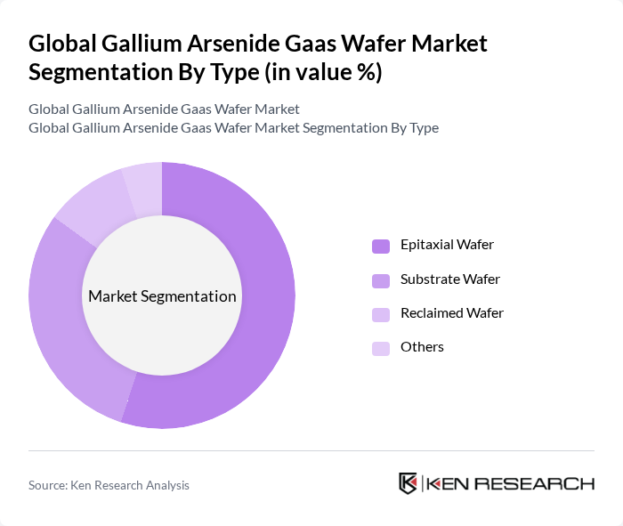
Global Gallium Arsenide Gaas Wafer Market segmentation by Type.

By End-User:The market is categorized into Telecommunications, Aerospace & Defense, Consumer Electronics, and Industrial Applications. The Telecommunications segment is dominant, driven by the increasing demand for mobile communication technologies, rapid deployment of 5G networks, and the proliferation of wireless infrastructure. Growth in this segment is fueled by the need for high-performance RF components and power amplifiers. The Aerospace & Defense segment also shows significant growth due to the rising demand for reliable, efficient electronic systems and radar technologies in defense applications. Consumer electronics and industrial applications continue to expand, supported by the integration of GaAs wafers in LEDs, sensors, and industrial automation .
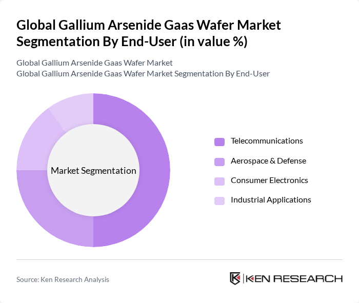
Global Gallium Arsenide Gaas Wafer Market segmentation by End-User.

Global Gallium Arsenide Gaas Wafer Market Competitive Landscape

The Global Gallium Arsenide GaAs Wafer Market is characterized by a dynamic mix of regional and international players. Leading participants such as AXT Inc., IQE PLC, Sumitomo Electric Industries, Ltd., Freiberger Compound Materials GmbH, II-VI Incorporated, Skyworks Solutions, Inc., NTT Advanced Technology Corporation, WIN Semiconductors Corp., Global Communication Semiconductors, LLC, Semiconductor Wafer Inc. (SWI), Xiamen Powerway Advanced Material Co., Ltd., Broadcom Inc., Qorvo, Inc., Panasonic Corporation, Mitsubishi Electric Corporation contribute to innovation, geographic expansion, and service delivery in this space.

AXT Inc.

1986

Fremont, California, USA

IQE PLC

1988

Cardiff, Wales, UK

Sumitomo Electric Industries, Ltd.

1897

Osaka, Japan

Freiberger Compound Materials GmbH

1992

Freiberg, Germany

II-VI Incorporated

1971

Saxonburg, Pennsylvania, USA

Company

Establishment Year

Headquarters

Group Size (Large, Medium, or Small as per industry convention)

Revenue Growth Rate (YoY %)

Market Share (%)

Geographic Footprint (Number of Countries/Regions Served)

Product Portfolio Breadth (Number of GaAs Wafer Types/Applications)

R&D Intensity (% of Revenue Spent on R&D)

Global Gallium Arsenide Gaas Wafer Market Industry Analysis

Growth Drivers

  • Increasing Demand for High-Efficiency Semiconductors:The global semiconductor market is projected to reach $1.1 trillion, driven by the demand for high-efficiency devices. Gallium arsenide (GaAs) wafers are crucial in producing high-performance semiconductors, particularly in telecommunications and consumer electronics. The increasing adoption of electric vehicles, which require advanced semiconductor technologies, is expected to contribute significantly to this demand, with the EV market anticipated to grow to 30 million units.
  • Expansion of 5G Infrastructure:The global investment in 5G infrastructure is expected to exceed $1.5 trillion, significantly boosting the demand for GaAs wafers. These wafers are essential for manufacturing high-frequency components used in 5G networks, such as power amplifiers and RF devices. As countries continue to roll out 5G networks, the need for efficient and reliable semiconductor solutions will drive the growth of the GaAs wafer market, particularly in regions like North America and Asia-Pacific.
  • Growth in Renewable Energy Applications:The renewable energy sector is projected to attract $3 trillion in investments, with solar energy leading the charge. GaAs wafers are increasingly used in photovoltaic cells due to their superior efficiency compared to silicon-based alternatives. The global solar power capacity is expected to reach 1,500 GW, creating substantial opportunities for GaAs wafer manufacturers to cater to the growing demand for high-efficiency solar panels.

Market Challenges

  • High Production Costs:The production of GaAs wafers is significantly more expensive than silicon wafers, with costs estimated at $120 per square inch compared to $25 for silicon. This high cost is primarily due to the complex manufacturing processes and the need for specialized equipment. As a result, many manufacturers face challenges in maintaining competitive pricing, which can hinder market growth, especially in price-sensitive regions.
  • Limited Availability of Raw Materials:The supply chain for gallium, a critical raw material for GaAs wafers, is constrained, with global production estimated at only 350 tons annually. This limited availability can lead to supply shortages and increased prices, impacting the overall production capacity of GaAs wafers. Additionally, geopolitical factors can further complicate the sourcing of gallium, posing a significant challenge for manufacturers in the industry.

Global Gallium Arsenide Gaas Wafer Market Future Outlook

The future of the GaAs wafer market appears promising, driven by technological advancements and increasing applications across various sectors. The integration of AI in semiconductor manufacturing is expected to enhance production efficiency and reduce costs. Furthermore, the trend towards miniaturization of electronic devices will continue to fuel demand for GaAs wafers, as they offer superior performance in compact designs. As sustainability becomes a priority, manufacturers are likely to adopt eco-friendly practices, aligning with global environmental goals.

Market Opportunities

  • Emerging Markets for Consumer Electronics:The consumer electronics market is projected to reach $1.8 trillion, with significant growth in regions like Asia-Pacific. This presents an opportunity for GaAs wafer manufacturers to expand their market presence by providing high-performance components for smartphones, tablets, and wearables, which increasingly rely on advanced semiconductor technologies.
  • Innovations in Photovoltaic Technologies:The solar energy sector is witnessing rapid innovations, with new photovoltaic technologies expected to enhance efficiency by 25%. GaAs wafers, known for their high efficiency, can play a pivotal role in these advancements, offering manufacturers a chance to capitalize on the growing demand for cutting-edge solar solutions in both residential and commercial markets.

Scope of the Report

SegmentSub-Segments
By Type

Epitaxial Wafer

Substrate Wafer

Reclaimed Wafer

Others

By End-User

Telecommunications

Aerospace & Defense

Consumer Electronics

Industrial Applications

By Application

RF Devices

Solar Cells

LED Technology

Laser Diodes

By Distribution Channel

Direct Sales

Distributors

Online Sales

By Region

North America

Europe

Asia-Pacific

Latin America

By Pricing Strategy

Premium Pricing

Competitive Pricing

Value-Based Pricing

By Technology

MOCVD (Metal-Organic Chemical Vapor Deposition)

LPE (Liquid Phase Epitaxy)

VGF (Vertical Gradient Freeze)

LEC (Liquid Encapsulated Czochralski)

CVD (Chemical Vapor Deposition)

Others

Key Target Audience

Investors and Venture Capitalist Firms

Government and Regulatory Bodies (e.g., U.S. Department of Energy, European Commission)

Manufacturers and Producers

Distributors and Retailers

Semiconductor Fabrication Facilities

Telecommunications Companies

Industry Associations (e.g., Semiconductor Industry Association)

Financial Institutions

Players Mentioned in the Report:

AXT Inc.

IQE PLC

Sumitomo Electric Industries, Ltd.

Freiberger Compound Materials GmbH

II-VI Incorporated

Skyworks Solutions, Inc.

NTT Advanced Technology Corporation

WIN Semiconductors Corp.

Global Communication Semiconductors, LLC

Semiconductor Wafer Inc. (SWI)

Xiamen Powerway Advanced Material Co., Ltd.

Broadcom Inc.

Qorvo, Inc.

Panasonic Corporation

Mitsubishi Electric Corporation

Table of Contents

Market Assessment Phase

1. Executive Summary and Approach


2. Global Gallium Arsenide Gaas Wafer Market Overview

2.1 Key Insights and Strategic Recommendations

2.2 Global Gallium Arsenide Gaas Wafer Market Overview

2.3 Definition and Scope

2.4 Evolution of Market Ecosystem

2.5 Timeline of Key Regulatory Milestones

2.6 Value Chain & Stakeholder Mapping

2.7 Business Cycle Analysis

2.8 Policy & Incentive Landscape


3. Global Gallium Arsenide Gaas Wafer Market Analysis

3.1 Growth Drivers

3.1.1 Increasing Demand for High-Efficiency Semiconductors
3.1.2 Expansion of 5G Infrastructure
3.1.3 Growth in Renewable Energy Applications
3.1.4 Advancements in Optoelectronic Devices

3.2 Market Challenges

3.2.1 High Production Costs
3.2.2 Limited Availability of Raw Materials
3.2.3 Stringent Environmental Regulations
3.2.4 Competition from Alternative Materials

3.3 Market Opportunities

3.3.1 Emerging Markets for Consumer Electronics
3.3.2 Innovations in Photovoltaic Technologies
3.3.3 Increased Investment in R&D
3.3.4 Collaborations with Tech Startups

3.4 Market Trends

3.4.1 Shift Towards Miniaturization of Devices
3.4.2 Rise of Smart Technologies
3.4.3 Integration of AI in Semiconductor Manufacturing
3.4.4 Focus on Sustainable Manufacturing Practices

3.5 Government Regulation

3.5.1 Regulations on Semiconductor Waste Management
3.5.2 Standards for Product Quality and Safety
3.5.3 Incentives for Renewable Energy Integration
3.5.4 Compliance with International Trade Agreements

4. SWOT Analysis


5. Stakeholder Analysis


6. Porter's Five Forces Analysis


7. Global Gallium Arsenide Gaas Wafer Market Market Size, 2019-2024

7.1 By Value

7.2 By Volume

7.3 By Average Selling Price


8. Global Gallium Arsenide Gaas Wafer Market Segmentation

8.1 By Type

8.1.1 Epitaxial Wafer
8.1.2 Substrate Wafer
8.1.3 Reclaimed Wafer
8.1.4 Others

8.2 By End-User

8.2.1 Telecommunications
8.2.2 Aerospace & Defense
8.2.3 Consumer Electronics
8.2.4 Industrial Applications

8.3 By Application

8.3.1 RF Devices
8.3.2 Solar Cells
8.3.3 LED Technology
8.3.4 Laser Diodes

8.4 By Distribution Channel

8.4.1 Direct Sales
8.4.2 Distributors
8.4.3 Online Sales

8.5 By Region

8.5.1 North America
8.5.2 Europe
8.5.3 Asia-Pacific
8.5.4 Latin America

8.6 By Pricing Strategy

8.6.1 Premium Pricing
8.6.2 Competitive Pricing
8.6.3 Value-Based Pricing

8.7 By Technology

8.7.1 MOCVD (Metal-Organic Chemical Vapor Deposition)
8.7.2 LPE (Liquid Phase Epitaxy)
8.7.3 VGF (Vertical Gradient Freeze)
8.7.4 LEC (Liquid Encapsulated Czochralski)
8.7.5 CVD (Chemical Vapor Deposition)
8.7.6 Others

9. Global Gallium Arsenide Gaas Wafer Market Competitive Analysis

9.1 Market Share of Key Players

9.2 KPIs for Cross Comparison of Key Players

9.2.1 Company Name
9.2.2 Group Size (Large, Medium, or Small as per industry convention)
9.2.3 Revenue Growth Rate (YoY %)
9.2.4 Market Share (%)
9.2.5 Geographic Footprint (Number of Countries/Regions Served)
9.2.6 Product Portfolio Breadth (Number of GaAs Wafer Types/Applications)
9.2.7 R&D Intensity (% of Revenue Spent on R&D)
9.2.8 Manufacturing Capacity (Annual Wafer Output, sq. inches or units)
9.2.9 Supply Chain Reliability (On-Time Delivery Rate %)
9.2.10 Customer Base (Number of Major OEM/ODM Clients)
9.2.11 Patent Holdings (Number of Relevant Patents)
9.2.12 Sustainability Score (Environmental Compliance, Certifications)
9.2.13 Innovation Rate (New Product Launches per Year)
9.2.14 Profit Margin (%)
9.2.15 Pricing Strategy (Premium, Competitive, Value-Based)

9.3 SWOT Analysis of Top Players

9.4 Pricing Analysis

9.5 Detailed Profile of Major Companies

9.5.1 AXT Inc.
9.5.2 IQE PLC
9.5.3 Sumitomo Electric Industries, Ltd.
9.5.4 Freiberger Compound Materials GmbH
9.5.5 II-VI Incorporated
9.5.6 Skyworks Solutions, Inc.
9.5.7 NTT Advanced Technology Corporation
9.5.8 WIN Semiconductors Corp.
9.5.9 Global Communication Semiconductors, LLC
9.5.10 Semiconductor Wafer Inc. (SWI)
9.5.11 Xiamen Powerway Advanced Material Co., Ltd.
9.5.12 Broadcom Inc.
9.5.13 Qorvo, Inc.
9.5.14 Panasonic Corporation
9.5.15 Mitsubishi Electric Corporation

10. Global Gallium Arsenide Gaas Wafer Market End-User Analysis

10.1 Procurement Behavior of Key Ministries

10.1.1 Government Contracts and Tenders
10.1.2 Budget Allocations for Technology
10.1.3 Compliance with National Standards

10.2 Corporate Spend on Infrastructure & Energy

10.2.1 Investment in Semiconductor Manufacturing
10.2.2 Funding for Renewable Energy Projects
10.2.3 Expenditure on R&D Initiatives

10.3 Pain Point Analysis by End-User Category

10.3.1 Supply Chain Disruptions
10.3.2 Cost Management Challenges
10.3.3 Technology Integration Issues

10.4 User Readiness for Adoption

10.4.1 Training and Skill Development Needs
10.4.2 Infrastructure Readiness
10.4.3 Awareness of Benefits

10.5 Post-Deployment ROI and Use Case Expansion

10.5.1 Performance Metrics Tracking
10.5.2 Scalability of Solutions
10.5.3 Long-term Cost Savings

11. Global Gallium Arsenide Gaas Wafer Market Future Size, 2025-2030

11.1 By Value

11.2 By Volume

11.3 By Average Selling Price


Go-To-Market Strategy Phase

1. Whitespace Analysis + Business Model Canvas

1.1 Market Gaps Identification

1.2 Value Proposition Development

1.3 Revenue Streams Analysis

1.4 Cost Structure Evaluation

1.5 Key Partnerships Exploration

1.6 Customer Segmentation

1.7 Channels of Distribution


2. Marketing and Positioning Recommendations

2.1 Branding Strategies

2.2 Product USPs

2.3 Target Market Identification

2.4 Communication Strategies

2.5 Digital Marketing Approaches


3. Distribution Plan

3.1 Urban Retail Strategies

3.2 Rural NGO Tie-ups

3.3 Online Distribution Channels

3.4 Direct Sales Approaches


4. Channel & Pricing Gaps

4.1 Underserved Routes

4.2 Pricing Bands Analysis

4.3 Competitor Pricing Strategies


5. Unmet Demand & Latent Needs

5.1 Category Gaps Identification

5.2 Consumer Segments Analysis

5.3 Emerging Trends Exploration


6. Customer Relationship

6.1 Loyalty Programs Development

6.2 After-sales Service Strategies

6.3 Customer Feedback Mechanisms


7. Value Proposition

7.1 Sustainability Initiatives

7.2 Integrated Supply Chains

7.3 Competitive Advantages


8. Key Activities

8.1 Regulatory Compliance

8.2 Branding Initiatives

8.3 Distribution Setup


9. Entry Strategy Evaluation

9.1 Domestic Market Entry Strategy

9.1.1 Product Mix Considerations
9.1.2 Pricing Band Strategies
9.1.3 Packaging Innovations

9.2 Export Entry Strategy

9.2.1 Target Countries Identification
9.2.2 Compliance Roadmap Development

10. Entry Mode Assessment

10.1 Joint Ventures

10.2 Greenfield Investments

10.3 Mergers & Acquisitions

10.4 Distributor Model Evaluation


11. Capital and Timeline Estimation

11.1 Capital Requirements Analysis

11.2 Timelines for Implementation


12. Control vs Risk Trade-Off

12.1 Ownership Considerations

12.2 Partnerships Evaluation


13. Profitability Outlook

13.1 Breakeven Analysis

13.2 Long-term Sustainability Strategies


14. Potential Partner List

14.1 Distributors Identification

14.2 Joint Ventures Opportunities

14.3 Acquisition Targets


15. Execution Roadmap

15.1 Phased Plan for Market Entry

15.1.1 Market Setup
15.1.2 Market Entry
15.1.3 Growth Acceleration
15.1.4 Scale & Stabilize

15.2 Key Activities and Milestones

15.2.1 Milestone Planning
15.2.2 Activity Tracking

Research Methodology

ApproachModellingSample

Phase 1: Approach1

Desk Research

  • Industry reports from semiconductor associations and market research firms
  • Technical papers and publications on GaAs wafer technology advancements
  • Market statistics from government databases and trade organizations

Primary Research

  • Interviews with R&D heads at leading semiconductor manufacturers
  • Surveys with procurement managers in the electronics and optoelectronics sectors
  • Field interviews with engineers specializing in wafer fabrication processes

Validation & Triangulation

  • Cross-validation of data from multiple industry sources and expert opinions
  • Triangulation of market size estimates using production, consumption, and trade data
  • Sanity checks through feedback from industry panels and focus groups

Phase 2: Market Size Estimation1

Top-down Assessment

  • Analysis of global semiconductor market growth trends and projections
  • Segmentation of GaAs wafer demand by application sectors such as telecommunications and solar energy
  • Incorporation of regional market dynamics and technological adoption rates

Bottom-up Modeling

  • Volume estimates based on production capacities of major GaAs wafer manufacturers
  • Cost analysis derived from raw material prices and manufacturing expenses
  • Estimation of market share based on sales data from key industry players

Forecasting & Scenario Analysis

  • Multi-variable regression analysis incorporating factors like technological advancements and market demand shifts
  • Scenario modeling based on potential regulatory changes and environmental considerations
  • Development of baseline, optimistic, and pessimistic forecasts through 2030

Phase 3: CATI Sample Composition1

Scope Item/SegmentSample SizeTarget Respondent Profiles
Telecommunications Applications60Product Managers, Technology Directors
Solar Energy Solutions50Project Engineers, Procurement Specialists
Consumer Electronics Manufacturing55Operations Managers, Supply Chain Analysts
Research & Development in Semiconductors40R&D Managers, Technical Leads
Wafer Fabrication Facilities45Manufacturing Engineers, Quality Control Managers

Frequently Asked Questions

What is the current value of the Global Gallium Arsenide (GaAs) Wafer Market?

The Global Gallium Arsenide Wafer Market is valued at approximately USD 670 million, reflecting a significant growth trend driven by the demand for high-performance electronic devices, particularly in telecommunications and consumer electronics.

What factors are driving the growth of the GaAs wafer market?

Which regions dominate the GaAs wafer market?

What are the main types of GaAs wafers available in the market?

Other Regional/Country Reports

UAE Gallium Arsenide Gaas Wafer MarketKSA Gallium Arsenide Gaas Wafer Market

Indonesia Gallium Arsenide Gaas Wafer Market

Malaysia Gallium Arsenide Gaas Wafer Market

APAC Gallium Arsenide Gaas Wafer Market

SEA Gallium Arsenide Gaas Wafer Market

Why Buy From Us?

Refine Robust Result (RRR) Framework

What makes us stand out is that our consultants follow Robust, Refine and Result (RRR) methodology. Robust for clear definitions, approaches and sanity checking, Refine for differentiating respondents' facts and opinions, and Result for presenting data with story.

Our Reach Is Unmatched

We have set a benchmark in the industry by offering our clients with syndicated and customized market research reports featuring coverage of entire market as well as meticulous research and analyst insights.

Shifting the Research Paradigm

While we don't replace traditional research, we flip the method upside down. Our dual approach of Top Bottom & Bottom Top ensures quality deliverable by not just verifying company fundamentals but also looking at the sector and macroeconomic factors.

More Insights-Better Decisions

With one step in the future, our research team constantly tries to show you the bigger picture. We help with some of the tough questions you may encounter along the way: How is the industry positioned? Best marketing channel? KPI's of competitors? By aligning every element, we help maximize success.

Transparency and Trust

Our report gives you instant access to the answers and sources that other companies might choose to hide. We elaborate each steps of research methodology we have used and showcase you the sample size to earn your trust.

Round the Clock Support

If you need any support, we are here! We pride ourselves on universe strength, data quality, and quick, friendly, and professional service.

Why Clients Choose Us?

400000+
Reports in repository
150+
Consulting projects a year
100+
Analysts
8000+
Client Queries in 2022