Global Wafer Prober Market

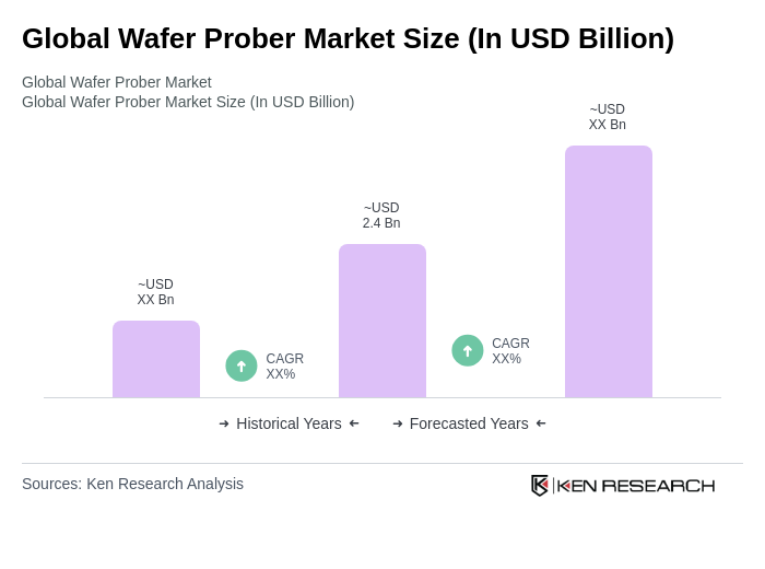
The Global Wafer Prober Market, valued at USD 2.4 billion, is growing due to rising semiconductor needs in consumer electronics, automotive, and 5G technologies.

Region:Global

Author(s):Geetanshi

Product Code:KRAA1188

Pages:99

Published On:August 2025
About the Report

Base Year 2024

Global Wafer Prober Market Overview

  • The Global Wafer Prober Market is valued at USD 2.4 billion, based on a five-year historical analysis. This growth is primarily driven by the increasing demand for semiconductor devices across various industries, including consumer electronics, automotive, and telecommunications. The rise in the adoption of advanced technologies such as 5G, IoT, and electric vehicles has further propelled the need for efficient wafer probing solutions, ensuring high-quality semiconductor manufacturing. Additionally, the proliferation of smartphones and wearable devices, as well as advancements in automotive electronics such as ADAS and infotainment systems, are significant contributors to market expansion .
  • Key players in this market include the United States, Japan, and South Korea, which dominate due to their strong semiconductor manufacturing capabilities and technological advancements. The presence of major semiconductor companies and research institutions in these regions fosters innovation and enhances the competitive landscape, making them pivotal in the global wafer prober market .
  • In 2023, the U.S. government implemented regulations aimed at enhancing semiconductor manufacturing capabilities, including the CHIPS Act, which allocates USD 52 billion for semiconductor research and development. This initiative is designed to boost domestic production and reduce reliance on foreign supply chains, thereby strengthening the overall semiconductor ecosystem .
Global Wafer Prober Market Size

Global Wafer Prober Market Segmentation

By Type:The market is segmented into Manual Probers, Semi-Automatic Probers, and Fully Automatic Probers. Among these, Fully Automatic Probers are leading the market due to their efficiency and precision in handling high-volume production. The trend towards automation in semiconductor manufacturing is driving the demand for fully automatic solutions, as they reduce human error and increase throughput. Fully automatic wafer probers are particularly favored in mass-production environments for their high precision and speed, while semi-automatic and manual probers are more commonly used in research, development, and low-volume production settings .
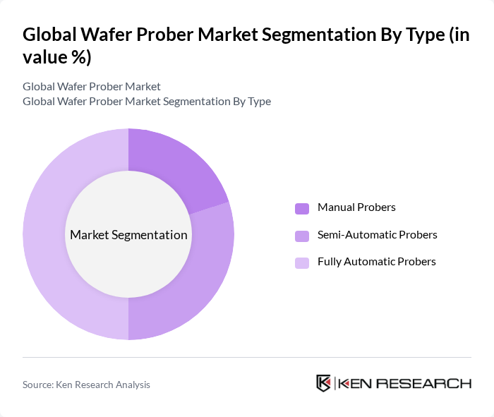
Global Wafer Prober Market segmentation by Type.

By End-User:The end-user segmentation includes Semiconductor Manufacturers, Research & Development Institutions, and Electronics & Device Manufacturers. Semiconductor Manufacturers dominate this segment, driven by the increasing demand for chips in various applications such as smartphones, automotive electronics, and industrial automation. The continuous innovation in semiconductor technology, particularly in advanced node manufacturing and integration of AI functionalities, further fuels the growth of this segment .

Global Wafer Prober Market segmentation by End-User.

Global Wafer Prober Market Competitive Landscape

The Global Wafer Prober Market is characterized by a dynamic mix of regional and international players. Leading participants such as Tokyo Electron Limited (TEL), Tokyo Seimitsu Co., Ltd. (Accretech), FormFactor, Inc., Micronics Japan Co., Ltd. (MJC), MPI Corporation, Wentworth Laboratories Ltd., Advantest Corporation, Chroma ATE Inc., SUSS MicroTec SE, Cohu, Inc., Lake Shore Cryotronics, Inc., ESDEMC Technology LLC, Hprobe, Shenzhen Sidea Semiconductor Co., Ltd., and Psaic (Precision Systems Industrial Co., Ltd.) contribute to innovation, geographic expansion, and service delivery in this space.

Tokyo Electron Limited (TEL)

1963

Tokyo, Japan

Tokyo Seimitsu Co., Ltd. (Accretech)

1949

Hachioji, Tokyo, Japan

FormFactor, Inc.

1993

Livermore, California, USA

Micronics Japan Co., Ltd. (MJC)

1970

Tokyo, Japan

MPI Corporation

1995

Hsinchu, Taiwan

Company

Establishment Year

Headquarters

Company Size (Large, Medium, Small)

Annual Revenue (USD Million)

Revenue Growth Rate (%)

Global Market Share (%)

Installed Base (Units)

R&D Expenditure (% of Revenue)

Global Wafer Prober Market Industry Analysis

Growth Drivers

  • Increasing Demand for Semiconductor Devices:The global semiconductor market is projected to reach $1 trillion in future, driven by the rising demand for consumer electronics, automotive applications, and industrial automation. In future, the semiconductor industry is expected to grow by approximately $100 billion, necessitating advanced wafer probing technologies to ensure quality and performance. This surge in demand directly influences the need for efficient wafer probers, which are essential for testing semiconductor devices before they are integrated into various applications.
  • Advancements in Wafer Probing Technology:The wafer probing technology landscape is evolving rapidly, with innovations such as high-speed probing and enhanced accuracy. In future, the market for advanced probing systems is anticipated to grow by $2 billion, reflecting the industry's shift towards more sophisticated testing solutions. These advancements are crucial for meeting the stringent quality standards required in semiconductor manufacturing, thereby driving the adoption of modern wafer probers across various sectors, including telecommunications and consumer electronics.
  • Rising Investment in R&D Activities:Global investments in semiconductor R&D are projected to exceed $40 billion in future, as companies strive to innovate and enhance their product offerings. This influx of funding is expected to foster the development of next-generation wafer probers that can handle complex testing requirements. As manufacturers seek to improve yield rates and reduce production costs, the demand for advanced probing solutions will continue to rise, further propelling market growth in the wafer prober sector.

Market Challenges

  • High Initial Investment Costs:The capital required to acquire advanced wafer probers can be substantial, often exceeding $1 million per unit. This high initial investment poses a significant barrier for smaller manufacturers and startups, limiting their ability to compete in the market. As the semiconductor industry continues to evolve, companies must weigh the costs against potential returns, which can hinder the adoption of new probing technologies and slow overall market growth.
  • Complexity of Probing Processes:The probing process involves intricate procedures that require specialized knowledge and training. In future, it is estimated that over 30% of semiconductor manufacturers will face challenges related to the complexity of these processes, leading to increased operational costs and potential delays in production. This complexity can deter companies from investing in advanced wafer probers, as they may struggle to find skilled personnel capable of operating and maintaining these sophisticated systems.

Global Wafer Prober Market Future Outlook

The future of the wafer prober market appears promising, driven by technological advancements and increasing demand for semiconductor devices. As industries such as automotive and telecommunications expand, the need for efficient testing solutions will grow. Additionally, the integration of artificial intelligence in manufacturing processes is expected to enhance operational efficiency. Companies that invest in innovative probing technologies will likely gain a competitive edge, positioning themselves favorably in a rapidly evolving market landscape.

Market Opportunities

  • Growth in Automotive Electronics:The automotive electronics market is projected to reach $400 billion in future, driven by the increasing adoption of electric vehicles and advanced driver-assistance systems. This growth presents significant opportunities for wafer probers, as manufacturers will require reliable testing solutions to ensure the performance and safety of electronic components used in vehicles.
  • Emergence of 5G Technology:The rollout of 5G technology is expected to create a demand for advanced semiconductor devices, with an estimated 1.5 billion 5G-enabled devices projected to be in use in future. This surge will necessitate enhanced wafer probing solutions to meet the stringent performance requirements of 5G applications, providing a lucrative opportunity for market players to innovate and expand their offerings.

Scope of the Report

SegmentSub-Segments
By Type

Manual Probers

Semi-Automatic Probers

Fully Automatic Probers

By End-User

Semiconductor Manufacturers

Research & Development Institutions

Electronics & Device Manufacturers

By Application

Wafer Testing (IC/Chip Testing)

Device Characterization

Failure Analysis

MEMS & Sensor Testing

By Component

Probe Cards

Probing Stations

Control & Automation Systems

Chuck Systems

By Sales Channel

Direct Sales

Distributors

Online Sales

By Region

North America

Europe

Asia Pacific

Latin America

Middle East & Africa

By Price Range

Low-End Probers

Mid-Range Probers

High-End Probers

Key Target Audience

Investors and Venture Capitalist Firms

Government and Regulatory Bodies (e.g., U.S. Department of Commerce, European Commission)

Manufacturers and Producers

Distributors and Retailers

Semiconductor Fabrication Facilities

Technology Providers

Industry Associations (e.g., SEMI, SIA)

Financial Institutions

Players Mentioned in the Report:

Tokyo Electron Limited (TEL)

Tokyo Seimitsu Co., Ltd. (Accretech)

FormFactor, Inc.

Micronics Japan Co., Ltd. (MJC)

MPI Corporation

Wentworth Laboratories Ltd.

Advantest Corporation

Chroma ATE Inc.

SUSS MicroTec SE

Cohu, Inc.

Lake Shore Cryotronics, Inc.

ESDEMC Technology LLC

Hprobe

Shenzhen Sidea Semiconductor Co., Ltd.

Psaic (Precision Systems Industrial Co., Ltd.)

Table of Contents

Market Assessment Phase

1. Executive Summary and Approach


2. Global Wafer Prober Market Overview

2.1 Key Insights and Strategic Recommendations

2.2 Global Wafer Prober Market Overview

2.3 Definition and Scope

2.4 Evolution of Market Ecosystem

2.5 Timeline of Key Regulatory Milestones

2.6 Value Chain & Stakeholder Mapping

2.7 Business Cycle Analysis

2.8 Policy & Incentive Landscape


3. Global Wafer Prober Market Analysis

3.1 Growth Drivers

3.1.1 Increasing Demand for Semiconductor Devices
3.1.2 Advancements in Wafer Probing Technology
3.1.3 Rising Investment in R&D Activities
3.1.4 Expansion of Electronics Manufacturing

3.2 Market Challenges

3.2.1 High Initial Investment Costs
3.2.2 Complexity of Probing Processes
3.2.3 Supply Chain Disruptions
3.2.4 Regulatory Compliance Issues

3.3 Market Opportunities

3.3.1 Growth in Automotive Electronics
3.3.2 Emergence of 5G Technology
3.3.3 Increasing Adoption of IoT Devices
3.3.4 Development of Advanced Packaging Solutions

3.4 Market Trends

3.4.1 Miniaturization of Electronic Components
3.4.2 Integration of AI in Wafer Probing
3.4.3 Shift Towards Automation in Manufacturing
3.4.4 Growing Focus on Sustainability

3.5 Government Regulation

3.5.1 Environmental Compliance Standards
3.5.2 Safety Regulations for Manufacturing
3.5.3 Export Control Regulations
3.5.4 Incentives for R&D Investments

4. SWOT Analysis


5. Stakeholder Analysis


6. Porter's Five Forces Analysis


7. Global Wafer Prober Market Market Size, 2019-2024

7.1 By Value

7.2 By Volume

7.3 By Average Selling Price


8. Global Wafer Prober Market Segmentation

8.1 By Type

8.1.1 Manual Probers
8.1.2 Semi-Automatic Probers
8.1.3 Fully Automatic Probers

8.2 By End-User

8.2.1 Semiconductor Manufacturers
8.2.2 Research & Development Institutions
8.2.3 Electronics & Device Manufacturers

8.3 By Application

8.3.1 Wafer Testing (IC/Chip Testing)
8.3.2 Device Characterization
8.3.3 Failure Analysis
8.3.4 MEMS & Sensor Testing

8.4 By Component

8.4.1 Probe Cards
8.4.2 Probing Stations
8.4.3 Control & Automation Systems
8.4.4 Chuck Systems

8.5 By Sales Channel

8.5.1 Direct Sales
8.5.2 Distributors
8.5.3 Online Sales

8.6 By Region

8.6.1 North America
8.6.2 Europe
8.6.3 Asia Pacific
8.6.4 Latin America
8.6.5 Middle East & Africa

8.7 By Price Range

8.7.1 Low-End Probers
8.7.2 Mid-Range Probers
8.7.3 High-End Probers

9. Global Wafer Prober Market Competitive Analysis

9.1 Market Share of Key Players

9.2 Cross Comparison of Key Players

9.2.1 Company Name
9.2.2 Company Size (Large, Medium, Small)
9.2.3 Annual Revenue (USD Million)
9.2.4 Revenue Growth Rate (%)
9.2.5 Global Market Share (%)
9.2.6 Installed Base (Units)
9.2.7 R&D Expenditure (% of Revenue)
9.2.8 Product Portfolio Breadth
9.2.9 Geographic Presence (Regions Served)
9.2.10 Customer Segments Served
9.2.11 Product Innovation Rate (New Launches/Year)
9.2.12 After-Sales Service Network Size
9.2.13 Operational Efficiency (Lead Time, Uptime %)
9.2.14 Pricing Strategy (Premium, Value, Volume)
9.2.15 Brand Recognition (Industry Awards, Rankings)

9.3 SWOT Analysis of Top Players

9.4 Pricing Analysis

9.5 Detailed Profile of Major Companies

9.5.1 Tokyo Electron Limited (TEL)
9.5.2 Tokyo Seimitsu Co., Ltd. (Accretech)
9.5.3 FormFactor, Inc.
9.5.4 Micronics Japan Co., Ltd. (MJC)
9.5.5 MPI Corporation
9.5.6 Wentworth Laboratories Ltd.
9.5.7 Advantest Corporation
9.5.8 Chroma ATE Inc.
9.5.9 SUSS MicroTec SE
9.5.10 Cohu, Inc.
9.5.11 Lake Shore Cryotronics, Inc.
9.5.12 ESDEMC Technology LLC
9.5.13 Hprobe
9.5.14 Shenzhen Sidea Semiconductor Co., Ltd.
9.5.15 Psaic (Precision Systems Industrial Co., Ltd.)

10. Global Wafer Prober Market End-User Analysis

10.1 Procurement Behavior of Key Ministries

10.1.1 Government Procurement Policies
10.1.2 Budget Allocations for Technology
10.1.3 Collaboration with Private Sector

10.2 Corporate Spend on Infrastructure & Energy

10.2.1 Investment in Semiconductor Facilities
10.2.2 Funding for R&D Initiatives
10.2.3 Expenditure on Probing Equipment

10.3 Pain Point Analysis by End-User Category

10.3.1 Equipment Reliability Issues
10.3.2 High Operational Costs
10.3.3 Need for Skilled Workforce

10.4 User Readiness for Adoption

10.4.1 Awareness of New Technologies
10.4.2 Training and Support Requirements
10.4.3 Financial Readiness for Investment

10.5 Post-Deployment ROI and Use Case Expansion

10.5.1 Measurement of Performance Metrics
10.5.2 Case Studies of Successful Implementations
10.5.3 Future Expansion Plans

11. Global Wafer Prober Market Future Size, 2025-2030

11.1 By Value

11.2 By Volume

11.3 By Average Selling Price


Go-To-Market Strategy Phase

1. Whitespace Analysis + Business Model Canvas

1.1 Market Gaps Identification

1.2 Value Proposition Development

1.3 Revenue Streams Analysis

1.4 Cost Structure Evaluation

1.5 Key Partnerships Exploration

1.6 Customer Segmentation

1.7 Channels of Distribution


2. Marketing and Positioning Recommendations

2.1 Branding Strategies

2.2 Product USPs

2.3 Target Market Identification

2.4 Communication Strategies

2.5 Digital Marketing Approaches


3. Distribution Plan

3.1 Urban Retail Strategies

3.2 Rural NGO Tie-Ups

3.3 Online Distribution Channels

3.4 Partnerships with Distributors


4. Channel & Pricing Gaps

4.1 Underserved Routes

4.2 Pricing Bands Analysis

4.3 Competitor Pricing Strategies


5. Unmet Demand & Latent Needs

5.1 Category Gaps Identification

5.2 Consumer Segments Analysis

5.3 Emerging Trends Exploration


6. Customer Relationship

6.1 Loyalty Programs

6.2 After-Sales Service

6.3 Customer Feedback Mechanisms


7. Value Proposition

7.1 Sustainability Initiatives

7.2 Integrated Supply Chains

7.3 Competitive Advantages


8. Key Activities

8.1 Regulatory Compliance

8.2 Branding Efforts

8.3 Distribution Setup


9. Entry Strategy Evaluation

9.1 Domestic Market Entry Strategy

9.1.1 Product Mix Considerations
9.1.2 Pricing Band Strategy
9.1.3 Packaging Solutions

9.2 Export Entry Strategy

9.2.1 Target Countries Identification
9.2.2 Compliance Roadmap Development

10. Entry Mode Assessment

10.1 Joint Ventures

10.2 Greenfield Investments

10.3 Mergers & Acquisitions

10.4 Distributor Model Evaluation


11. Capital and Timeline Estimation

11.1 Capital Requirements

11.2 Timelines for Implementation


12. Control vs Risk Trade-Off

12.1 Ownership Considerations

12.2 Partnerships Evaluation


13. Profitability Outlook

13.1 Breakeven Analysis

13.2 Long-Term Sustainability Strategies


14. Potential Partner List

14.1 Distributors

14.2 Joint Ventures

14.3 Acquisition Targets


15. Execution Roadmap

15.1 Phased Plan for Market Entry

15.1.1 Market Setup
15.1.2 Market Entry
15.1.3 Growth Acceleration
15.1.4 Scale & Stabilize

15.2 Key Activities and Milestones

15.2.1 Milestone Planning
15.2.2 Activity Scheduling

Research Methodology

ApproachModellingSample

Phase 1: Approach1

Desk Research

  • Industry reports from semiconductor associations and market research firms
  • Technical papers and publications from leading universities and research institutions
  • Market analysis from government publications and trade statistics

Primary Research

  • Interviews with engineers and product managers at semiconductor manufacturing companies
  • Surveys with procurement specialists in the wafer prober supply chain
  • Field interviews with technicians operating wafer probers in production environments

Validation & Triangulation

  • Cross-validation of data from multiple industry sources and expert opinions
  • Triangulation of market size estimates using historical sales data and growth trends
  • Sanity checks through expert panel discussions and feedback sessions

Phase 2: Market Size Estimation1

Top-down Assessment

  • Analysis of global semiconductor market growth and its impact on wafer prober demand
  • Segmentation of the market by application areas such as memory, logic, and RF devices
  • Incorporation of regional market dynamics and technological advancements

Bottom-up Modeling

  • Estimation of sales volume based on unit sales from leading wafer prober manufacturers
  • Operational cost analysis derived from pricing models of wafer probers
  • Volume x price calculations to derive revenue projections for different market segments

Forecasting & Scenario Analysis

  • Multi-variable regression analysis incorporating factors like semiconductor demand and technological shifts
  • Scenario modeling based on potential market disruptions and emerging technologies
  • Baseline, optimistic, and pessimistic forecasts through 2030 based on market trends

Phase 3: CATI Sample Composition1

Scope Item/SegmentSample SizeTarget Respondent Profiles
Memory Chip Manufacturing100Process Engineers, Production Managers
Logic Device Production80Quality Assurance Managers, Equipment Technicians
RF Device Testing60Test Engineers, R&D Managers
Wafer Prober Suppliers50Sales Directors, Product Development Engineers
Semiconductor Equipment Distributors40Supply Chain Managers, Business Development Executives

Frequently Asked Questions

What is the current value of the Global Wafer Prober Market?

The Global Wafer Prober Market is valued at approximately USD 2.4 billion, reflecting a significant growth trend driven by the increasing demand for semiconductor devices across various industries, including consumer electronics, automotive, and telecommunications.

What factors are driving the growth of the Global Wafer Prober Market?

Which regions dominate the Global Wafer Prober Market?

What types of wafer probers are available in the market?

Other Regional/Country Reports

Indonesia Global Wafer Prober Market

Malaysia Global Wafer Prober Market

KSA Global Wafer Prober Market

APAC Global Wafer Prober Market

SEA Global Wafer Prober Market

Vietnam Global Wafer Prober Market

Why Buy From Us?

Refine Robust Result (RRR) Framework

What makes us stand out is that our consultants follow Robust, Refine and Result (RRR) methodology. Robust for clear definitions, approaches and sanity checking, Refine for differentiating respondents' facts and opinions, and Result for presenting data with story.

Our Reach Is Unmatched

We have set a benchmark in the industry by offering our clients with syndicated and customized market research reports featuring coverage of entire market as well as meticulous research and analyst insights.

Shifting the Research Paradigm

While we don't replace traditional research, we flip the method upside down. Our dual approach of Top Bottom & Bottom Top ensures quality deliverable by not just verifying company fundamentals but also looking at the sector and macroeconomic factors.

More Insights-Better Decisions

With one step in the future, our research team constantly tries to show you the bigger picture. We help with some of the tough questions you may encounter along the way: How is the industry positioned? Best marketing channel? KPI's of competitors? By aligning every element, we help maximize success.

Transparency and Trust

Our report gives you instant access to the answers and sources that other companies might choose to hide. We elaborate each steps of research methodology we have used and showcase you the sample size to earn your trust.

Round the Clock Support

If you need any support, we are here! We pride ourselves on universe strength, data quality, and quick, friendly, and professional service.

Why Clients Choose Us?

400000+
Reports in repository
150+
Consulting projects a year
100+
Analysts
8000+
Client Queries in 2022