About the Report
Base Year 2024Global Photomask Market Overview
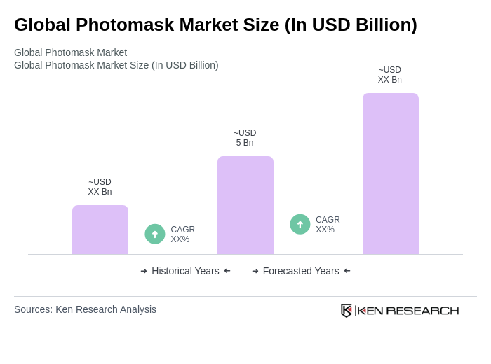
- The Global Photomask Market is valued at USD 5 billion, based on a five-year historical analysis. This growth is primarily driven by the increasing demand for advanced semiconductor manufacturing technologies, particularly in the production of integrated circuits and displays. The rise in consumer electronics and the proliferation of IoT devices have significantly contributed to the market's expansion.
- Key players in this market include the United States, Japan, and South Korea, which dominate due to their advanced technological capabilities and strong semiconductor manufacturing ecosystems. The presence of major foundries and research institutions in these regions fosters innovation and enhances the competitive landscape.
- In 2023, the U.S. government implemented regulations to support the semiconductor industry, including the CHIPS Act, which allocates USD 52 billion for semiconductor research and manufacturing. This initiative aims to bolster domestic production and reduce reliance on foreign supply chains, thereby enhancing the competitiveness of the U.S. photomask market.

Global Photomask Market Segmentation
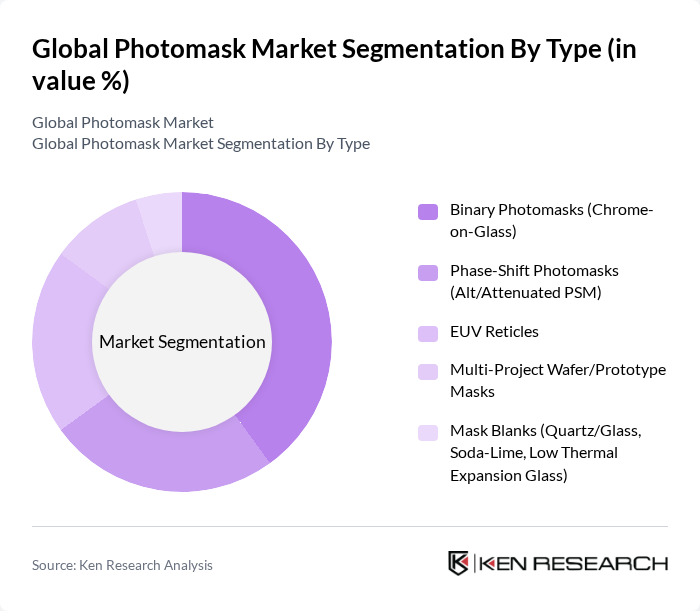
By Type:The photomask market is segmented into various types, including Binary Photomasks (Chrome-on-Glass), Phase-Shift Photomasks (Alt/Attenuated PSM), EUV Reticles, Multi-Project Wafer/Prototype Masks, and Mask Blanks (Quartz/Glass, Soda-Lime, Low Thermal Expansion Glass). Among these, Binary Photomasks are the most widely used due to their cost-effectiveness and suitability for a range of applications in semiconductor manufacturing.

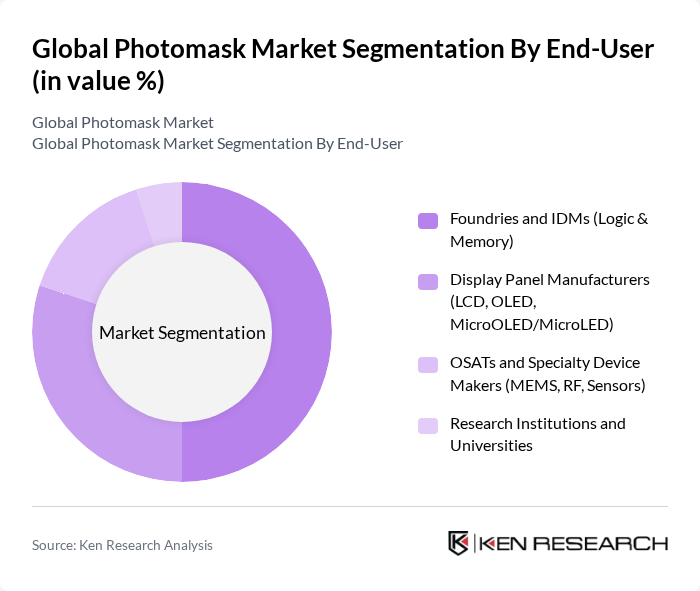
By End-User:The end-user segmentation includes Foundries and IDMs (Logic & Memory), Display Panel Manufacturers (LCD, OLED, MicroOLED/MicroLED), OSATs and Specialty Device Makers (MEMS, RF, Sensors), and Research Institutions and Universities. Foundries and IDMs dominate the market due to the high volume of photomasks required for logic and memory chip production, driven by the increasing demand for advanced computing and mobile devices.

Global Photomask Market Competitive Landscape
The Global Photomask Market is characterized by a dynamic mix of regional and international players. Leading participants such as Photronics, Inc., HOYA Corporation (Mask Blanks), Toppan Photomasks, Inc. (a division of TOPPAN Holdings), Dai Nippon Printing Co., Ltd. (DNP), SK-Electronics Co., Ltd., Taiwan Mask Corporation (TMC), Compugraphics International Ltd. (Photomask solutions), LG Innotek Co., Ltd. (Display photomasks), Lasertec Corporation (Mask inspection/metrology), ASML Holding N.V. (EUV systems and computational lithography), KLA Corporation (Reticle inspection), Canon Inc. (Lithography and mask aligners), Nikon Corporation (Lithography equipment), Xinyaqiang Silicon Chemistry Co., Ltd. (Mask materials), and Qingdao UPM Photomask Co., Ltd. contribute to innovation, geographic expansion, and service delivery in this space.
Global Photomask Market Industry Analysis
Growth Drivers
- Increasing Demand for Advanced Semiconductor Technologies:The global semiconductor industry is projected to reach one trillion USD by future, driven by innovations in AI, IoT, and 5G technologies. In future, the demand for advanced photomasks is expected to surge, with an estimated 20% increase in production capacity to meet the needs of cutting-edge semiconductor fabrication processes. This growth is fueled by the rising complexity of chips, which require more sophisticated photomask solutions to achieve smaller feature sizes and higher performance.
- Growth in Consumer Electronics Market:The consumer electronics market is anticipated to grow to one point five trillion USD in future, with significant contributions from smartphones, tablets, and wearables. This surge is expected to drive the demand for photomasks, as manufacturers require high-quality semiconductor components for these devices. The increasing adoption of smart devices, projected to reach thirty billion units globally by future, will further enhance the need for advanced photomask technologies to support the production of efficient and powerful chips.
- Expansion of 5G Technology:The global rollout of 5G technology is set to create a market worth seven hundred billion USD by future, significantly impacting the photomask industry. As telecom companies invest heavily in infrastructure, the demand for high-performance semiconductors will rise, necessitating advanced photomasks. The expected increase in data traffic, projected to reach four point five zettabytes per year, will drive semiconductor manufacturers to adopt innovative photomask solutions to enhance chip performance and efficiency.
Market Challenges
- High Manufacturing Costs:The production of photomasks involves significant capital investment, with costs reaching up to one million USD per mask for advanced technologies. This high cost can deter smaller manufacturers from entering the market, limiting competition and innovation. Additionally, the rising prices of raw materials, such as quartz and photoresists, are expected to increase overall production costs, impacting profit margins for photomask producers in future.
- Supply Chain Disruptions:The photomask industry is vulnerable to supply chain disruptions, as seen during the COVID-19 pandemic, which caused delays and shortages in critical materials. In future, ongoing geopolitical tensions and trade restrictions may exacerbate these challenges, leading to increased lead times and costs. Manufacturers may face difficulties sourcing essential components, which could hinder production capabilities and affect the overall market stability.
Global Photomask Market Future Outlook
The future of the photomask market appears promising, driven by technological advancements and increasing demand across various sectors. As semiconductor manufacturers continue to innovate, the integration of EUV lithography and smaller feature sizes will become more prevalent. Additionally, the focus on sustainability will push companies to develop eco-friendly photomasks, aligning with global environmental goals. The expansion into emerging markets will also present new opportunities for growth, as these regions adopt advanced technologies and increase their semiconductor production capabilities.
Market Opportunities
- Adoption of AI and Machine Learning in Manufacturing:The integration of AI and machine learning in photomask manufacturing processes is expected to enhance efficiency and reduce defects. By future, companies implementing these technologies could see a 15% reduction in production time, leading to cost savings and improved product quality. This trend presents a significant opportunity for photomask manufacturers to innovate and stay competitive in a rapidly evolving market.
- Development of Eco-Friendly Photomasks:As environmental concerns grow, the demand for eco-friendly photomasks is expected to rise. Manufacturers focusing on sustainable materials and processes could capture a significant share of the market, with projections indicating a potential 10% increase in sales for eco-friendly products by future. This shift not only aligns with global sustainability goals but also appeals to environmentally conscious consumers and businesses.
Scope of the Report
| Segment | Sub-Segments |
|---|---|
| By Type | Binary Photomasks (Chrome-on-Glass) Phase-Shift Photomasks (Alt/Attenuated PSM) EUV Reticles Multi-Project Wafer/Prototype Masks Mask Blanks (Quartz/Glass, Soda-Lime, Low Thermal Expansion Glass) |
| By End-User | Foundries and IDMs (Logic & Memory) Display Panel Manufacturers (LCD, OLED, MicroOLED/MicroLED) OSATs and Specialty Device Makers (MEMS, RF, Sensors) Research Institutions and Universities |
| By Application | Integrated Circuits (Logic, DRAM, NAND) Flat Panel Displays MEMS and Sensors Photonics and Advanced Packaging (RDL/Interposers) |
| By Sales Channel | Direct (Captive and Contract) Sales Authorized Distributors/Agents Strategic Supply Agreements/Long-Term Agreements (LTAs) |
| By Region | North America Europe Asia-Pacific Middle East & Africa Latin America |
| By Technology Node | Sub-20nm (EUV/ArF Immersion) –65nm (ArF/KrF) ?90nm (Legacy/Analog/Power/Discrete) |
| By Others | Custom/One-off Mask Services Niche Applications (Compound Semiconductors, Power, SiC/GaN) Emerging Technologies (MicroLED, Advanced Packaging, EUV High-NA) |
Key Target Audience
Investors and Venture Capitalist Firms
Government and Regulatory Bodies (e.g., U.S. Department of Commerce, European Commission)
Manufacturers and Producers
Distributors and Retailers
Semiconductor Fabrication Facilities
Technology Providers
Industry Associations (e.g., SEMI, SIA)
Financial Institutions
Players Mentioned in the Report:
Photronics, Inc.
HOYA Corporation (Mask Blanks)
Toppan Photomasks, Inc. (a division of TOPPAN Holdings)
Dai Nippon Printing Co., Ltd. (DNP)
SK-Electronics Co., Ltd.
Taiwan Mask Corporation (TMC)
Compugraphics International Ltd. (Photomask solutions)
LG Innotek Co., Ltd. (Display photomasks)
Lasertec Corporation (Mask inspection/metrology)
ASML Holding N.V. (EUV systems and computational lithography)
KLA Corporation (Reticle inspection)
Canon Inc. (Lithography and mask aligners)
Nikon Corporation (Lithography equipment)
Xinyaqiang Silicon Chemistry Co., Ltd. (Mask materials)
Qingdao UPM Photomask Co., Ltd.
Table of Contents
Market Assessment Phase
1. Executive Summary and Approach
2. Global Photomask Market Overview
2.1 Key Insights and Strategic Recommendations
2.2 Global Photomask Market Overview
2.3 Definition and Scope
2.4 Evolution of Market Ecosystem
2.5 Timeline of Key Regulatory Milestones
2.6 Value Chain & Stakeholder Mapping
2.7 Business Cycle Analysis
2.8 Policy & Incentive Landscape
3. Global Photomask Market Analysis
3.1 Growth Drivers
3.1.1 Increasing Demand for Advanced Semiconductor Technologies
3.1.2 Growth in Consumer Electronics Market
3.1.3 Expansion of 5G Technology
3.1.4 Rising Investment in Research and Development
3.2 Market Challenges
3.2.1 High Manufacturing Costs
3.2.2 Supply Chain Disruptions
3.2.3 Rapid Technological Changes
3.2.4 Limited Availability of Skilled Workforce
3.3 Market Opportunities
3.3.1 Adoption of AI and Machine Learning in Manufacturing
3.3.2 Growth in Automotive Electronics
3.3.3 Development of Eco-Friendly Photomasks
3.3.4 Expansion into Emerging Markets
3.4 Market Trends
3.4.1 Shift Towards Smaller Feature Sizes
3.4.2 Increasing Use of EUV Lithography
3.4.3 Integration of IoT in Semiconductor Manufacturing
3.4.4 Focus on Sustainability and Green Manufacturing
3.5 Government Regulation
3.5.1 Compliance with Environmental Standards
3.5.2 Export Control Regulations
3.5.3 Safety and Health Regulations
3.5.4 Intellectual Property Protection Laws
4. SWOT Analysis
5. Stakeholder Analysis
6. Porter's Five Forces Analysis
7. Global Photomask Market Market Size, 2019-2024
7.1 By Value
7.2 By Volume
7.3 By Average Selling Price
8. Global Photomask Market Segmentation
8.1 By Type
8.1.1 Binary Photomasks (Chrome-on-Glass)
8.1.2 Phase-Shift Photomasks (Alt/Attenuated PSM)
8.1.3 EUV Reticles
8.1.4 Multi-Project Wafer/Prototype Masks
8.1.5 Mask Blanks (Quartz/Glass, Soda-Lime, Low Thermal Expansion Glass)
8.2 By End-User
8.2.1 Foundries and IDMs (Logic & Memory)
8.2.2 Display Panel Manufacturers (LCD, OLED, MicroOLED/MicroLED)
8.2.3 OSATs and Specialty Device Makers (MEMS, RF, Sensors)
8.2.4 Research Institutions and Universities
8.3 By Application
8.3.1 Integrated Circuits (Logic, DRAM, NAND)
8.3.2 Flat Panel Displays
8.3.3 MEMS and Sensors
8.3.4 Photonics and Advanced Packaging (RDL/Interposers)
8.4 By Sales Channel
8.4.1 Direct (Captive and Contract) Sales
8.4.2 Authorized Distributors/Agents
8.4.3 Strategic Supply Agreements/Long-Term Agreements (LTAs)
8.5 By Region
8.5.1 North America
8.5.2 Europe
8.5.3 Asia-Pacific
8.5.4 Middle East & Africa
8.5.5 Latin America
8.6 By Technology Node
8.6.1 Sub-20nm (EUV/ArF Immersion)
8.6.2 20–65nm (ArF/KrF)
8.6.3 ?90nm (Legacy/Analog/Power/Discrete)
8.7 Others
8.7.1 Custom/One-off Mask Services
8.7.2 Niche Applications (Compound Semiconductors, Power, SiC/GaN)
8.7.3 Emerging Technologies (MicroLED, Advanced Packaging, EUV High-NA)
9. Global Photomask Market Competitive Analysis
9.1 Market Share of Key Players
9.2 Cross Comparison of Key Players
9.2.1 Company Name
9.2.2 Group Size (Pure-Play Mask Shop vs Captive vs Equipment/Materials)
9.2.3 Photomask Revenue (USD, latest FY)
9.2.4 Mask Capacity (plates/month or reticles/month)
9.2.5 EUV Capability (Yes/No; EUV layers supported; pellicle readiness)
9.2.6 Technology Coverage (EUV, ArF immersion, KrF, i-line)
9.2.7 Utilization Rate (%)
9.2.8 ASP per Mask/Reticle (by node where available)
9.2.9 Lead Time (days) and Yield (%)
9.2.10 Customer Mix (Foundry/IDM vs Display vs MEMS %)
9.2.11 Geographic Footprint (fabs/shops by region)
9.2.12 R&D Intensity (% of revenue) and IP Portfolio (patents)
9.2.13 Strategic Partnerships/LTAs (with foundries, display makers)
9.2.14 On-time Delivery & Defect Density (DPPM)
9.3 SWOT Analysis of Top Players
9.4 Pricing Analysis
9.5 Detailed Profile of Major Companies
9.5.1 Photronics, Inc.
9.5.2 HOYA Corporation (Mask Blanks)
9.5.3 Toppan Photomasks, Inc. (a division of TOPPAN Holdings)
9.5.4 Dai Nippon Printing Co., Ltd. (DNP)
9.5.5 SK-Electronics Co., Ltd.
9.5.6 Taiwan Mask Corporation (TMC)
9.5.7 Compugraphics International Ltd. (Photomask solutions)
9.5.8 LG Innotek Co., Ltd. (Display photomasks)
9.5.9 Lasertec Corporation (Mask inspection/metrology)
9.5.10 ASML Holding N.V. (EUV systems and computational lithography)
9.5.11 KLA Corporation (Reticle inspection)
9.5.12 Canon Inc. (Lithography and mask aligners)
9.5.13 Nikon Corporation (Lithography equipment)
9.5.14 Xinyaqiang Silicon Chemistry Co., Ltd. (Mask materials)
9.5.15 Qingdao UPM Photomask Co., Ltd.
10. Global Photomask Market End-User Analysis
10.1 Procurement Behavior of Key Ministries
10.1.1 Budget Allocation Trends
10.1.2 Decision-Making Processes
10.1.3 Supplier Selection Criteria
10.2 Corporate Spend on Infrastructure & Energy
10.2.1 Investment Priorities
10.2.2 Cost Management Strategies
10.2.3 Long-Term Financial Planning
10.3 Pain Point Analysis by End-User Category
10.3.1 Supply Chain Disruptions
10.3.2 Quality Assurance Issues
10.3.3 Technology Integration Challenges
10.4 User Readiness for Adoption
10.4.1 Training and Support Needs
10.4.2 Infrastructure Readiness
10.4.3 Change Management Strategies
10.5 Post-Deployment ROI and Use Case Expansion
10.5.1 Performance Metrics
10.5.2 Scalability Considerations
10.5.3 Future Investment Opportunities
11. Global Photomask Market Future Size, 2025-2030
11.1 By Value
11.2 By Volume
11.3 By Average Selling Price
Go-To-Market Strategy Phase
1. Whitespace Analysis + Business Model Canvas
1.1 Market Gaps Identification
1.2 Value Proposition Development
1.3 Revenue Streams Analysis
1.4 Customer Segmentation
1.5 Key Partnerships
1.6 Cost Structure Analysis
1.7 Competitive Advantage
2. Marketing and Positioning Recommendations
2.1 Branding Strategies
2.2 Product USPs
2.3 Target Market Identification
2.4 Communication Strategies
2.5 Digital Marketing Approaches
3. Distribution Plan
3.1 Urban Retail Strategies
3.2 Rural NGO Tie-Ups
3.3 E-commerce Integration
3.4 Logistics and Supply Chain Management
4. Channel & Pricing Gaps
4.1 Underserved Routes
4.2 Pricing Bands Analysis
4.3 Competitor Pricing Strategies
5. Unmet Demand & Latent Needs
5.1 Category Gaps
5.2 Consumer Segments Analysis
5.3 Emerging Trends Identification
6. Customer Relationship
6.1 Loyalty Programs
6.2 After-sales Service
6.3 Customer Feedback Mechanisms
7. Value Proposition
7.1 Sustainability Initiatives
7.2 Integrated Supply Chains
7.3 Customer-Centric Innovations
8. Key Activities
8.1 Regulatory Compliance
8.2 Branding Efforts
8.3 Distribution Setup
9. Entry Strategy Evaluation
9.1 Domestic Market Entry Strategy
9.1.1 Product Mix Considerations
9.1.2 Pricing Band Analysis
9.1.3 Packaging Strategies
9.2 Export Entry Strategy
9.2.1 Target Countries Identification
9.2.2 Compliance Roadmap Development
10. Entry Mode Assessment
10.1 Joint Ventures
10.2 Greenfield Investments
10.3 Mergers & Acquisitions
10.4 Distributor Model Evaluation
11. Capital and Timeline Estimation
11.1 Capital Requirements
11.2 Timelines for Implementation
12. Control vs Risk Trade-Off
12.1 Ownership Considerations
12.2 Partnerships Evaluation
13. Profitability Outlook
13.1 Breakeven Analysis
13.2 Long-term Sustainability Strategies
14. Potential Partner List
14.1 Distributors
14.2 Joint Ventures
14.3 Acquisition Targets
15. Execution Roadmap
15.1 Phased Plan for Market Entry
15.1.1 Market Setup
15.1.2 Market Entry
15.1.3 Growth Acceleration
15.1.4 Scale & Stabilize
15.2 Key Activities and Milestones
15.2.1 Milestone Planning
15.2.2 Activity Tracking
Research Methodology
Phase 1: Approach1
Desk Research
- Industry reports from semiconductor associations and photomask manufacturers
- Market analysis publications focusing on photomask technology trends
- Government publications and trade statistics related to semiconductor manufacturing
Primary Research
- Interviews with R&D heads at leading semiconductor firms
- Surveys with procurement managers in photomask production
- Field interviews with engineers specializing in photomask design and fabrication
Validation & Triangulation
- Cross-validation of market data through multiple industry sources
- Triangulation of findings from primary interviews and secondary data
- Sanity checks conducted through expert panels comprising industry veterans
Phase 2: Market Size Estimation1
Top-down Assessment
- Analysis of global semiconductor market size to estimate photomask demand
- Segmentation by technology node and application areas (e.g., memory, logic)
- Incorporation of trends in advanced packaging and 5G technology adoption
Bottom-up Modeling
- Volume estimates based on production capacities of major photomask manufacturers
- Cost analysis derived from pricing models of photomask products
- Calculation of market size based on unit sales and average selling prices
Forecasting & Scenario Analysis
- Multi-variable regression analysis incorporating technology adoption rates
- Scenario modeling based on shifts in semiconductor manufacturing processes
- Baseline, optimistic, and pessimistic forecasts through 2030
Phase 3: CATI Sample Composition1
| Scope Item/Segment | Sample Size | Target Respondent Profiles |
|---|---|---|
| Semiconductor Manufacturing Firms | 120 | Production Managers, Process Engineers |
| Photomask Suppliers | 90 | Sales Directors, Product Managers |
| Research Institutions | 60 | Research Scientists, Technology Analysts |
| End-User Industries (e.g., Consumer Electronics) | 60 | Product Development Managers, Supply Chain Analysts |
| Industry Associations | 40 | Policy Makers, Industry Experts |
Frequently Asked Questions
What is the current value of the Global Photomask Market?
The Global Photomask Market is valued at approximately USD 5 billion, driven by the increasing demand for advanced semiconductor manufacturing technologies, particularly in integrated circuits and display production.